ENGR433 Spring 2023
Homework 3
Name: Cheyenne Tucson
Email: crtucson@fortlewis.edu
Combinational Logic Blocks
Task 1
For the first task, both a Half-Adder and Full-Adder (1-bit) were simulated in Vivado.
The Full-Adder was simulated two different versions: one that implements a For Loop,
and one that has the bit combinations hard-coded into the script.
The Verilog scripts and simulation results for each can be found in PDF 1.
PDF 1. This is a PDF that contains all the screen-snips for the half and full adder simulations for Task 1.
Task 2
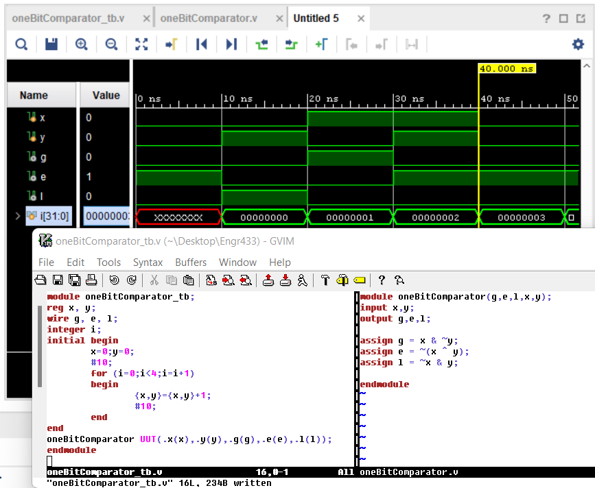
As the second task, a 1-bit comparator was described with Verilog. Once the testbench script was constructed,
a simulation was ran. The results along with both the testbench and description scripts can be seen in Figure 1 below.
Figure 1. A screen snip of the comparator simulation in Vivado and the Verilog scripts.
Task 3
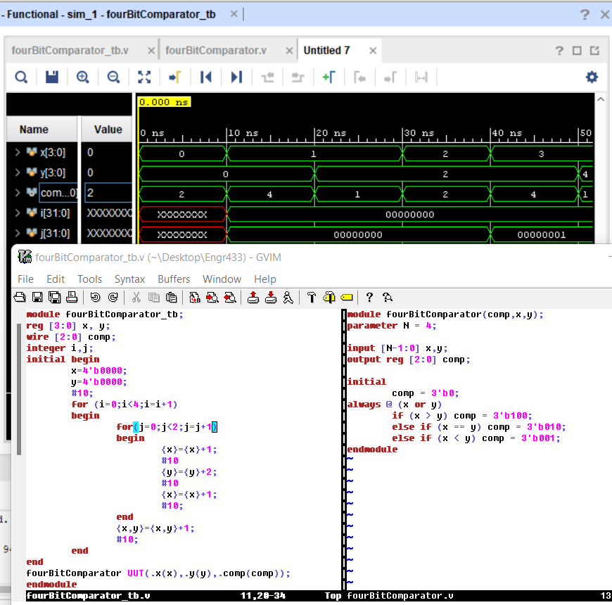
For the third task, another comparator was described and simulated; however, this time it is a 4-bit comparator.
This implements an If Statement in Verilog, which is another feature commonly found in Object Oriented Programming.
This 4-bit comparator takes two vectors of 4-bits each and determines whether the first vector is greater than, equal to,
or less than the second vector. The output of this comparator is also a vector of 3 elements, with element 0 corresponding
to corresponding to "less than," element 1 corresponding to "equal to," and the final element corresponding to "greater than."
Figure 2. A screen-snip of the behavior simulation ran in Vivado and code demonstrating the 4-bit comparator circuit.
a '1' in the 'comp' line indicates that vector x is less-than vector y; a '2' in the 'comp' line indicates the two vectors are equal;
a '4' in the 'comp' line indicates that vector x is greater-than vector y.
The simulation results and Verilog scripts can be seen in Figure 2 above.
Task 4
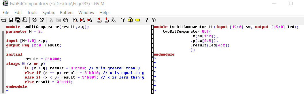
The next task involves implementing a comparator on the FPGA. This was done with a 4 switches and 3 LEDs:
two switches per input with MSB on the left, and LSB on the right; three LEDs are used to indicate from right
to left whether x is greater-than, equal-to, or less-than y.
Figure 3. The screen-snip of the Verilog scripts used to implement the 2-bit comparator on the FPGA. Video 1. The recorded demonstration of the comparator implemented on the FPGA.
Task 5
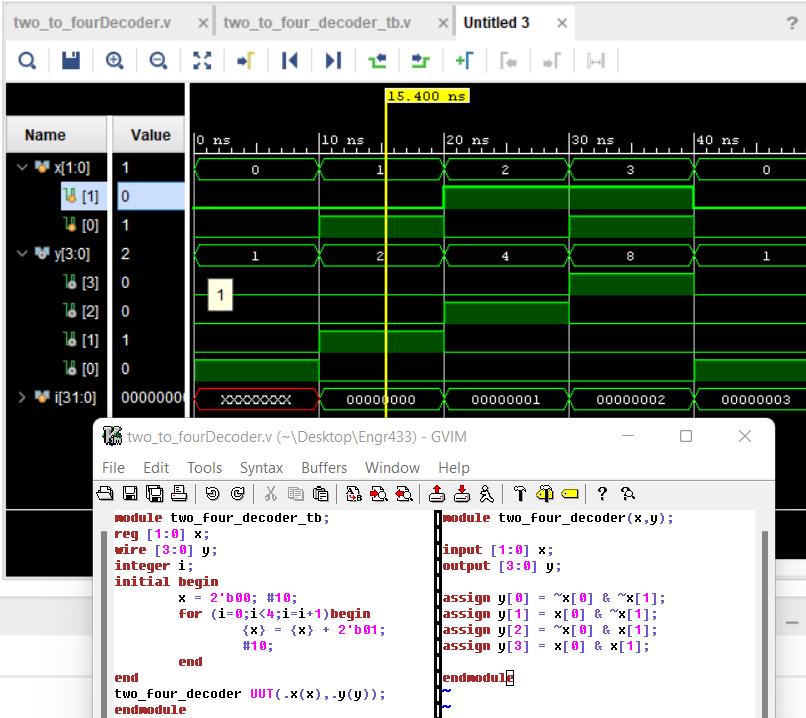
After the 2-bit comparator was implemented on the FPGA, a testbench script for a decoder was written,
and the decoder was simulated in Vivado. The results and code used for the simulation can be found below
in Figure 4.
Figure 4. The screen-snip of the Verilog scripts used to simulate the decoder in Vivado.
Task 6
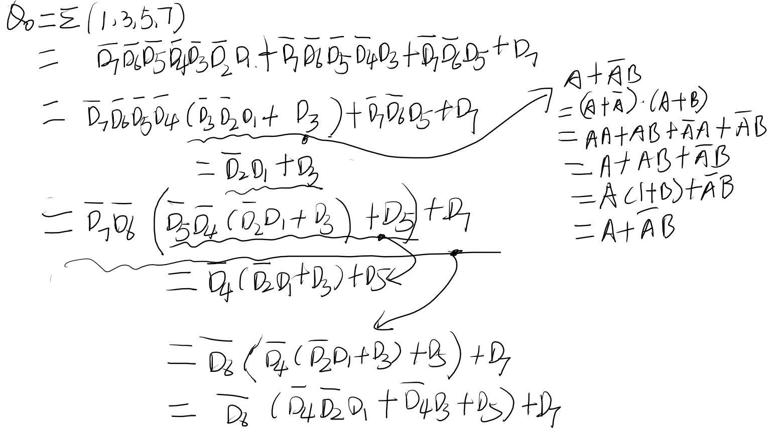
A decoder's compliment is an encoder. After the decoder was simulated for Task 5, code for an 8x3 Priority Encoder
was simulated in Vivado. To do so, the output conditions were derived from the truth table
of the encoder, particularly looking at the state of the 8 input bits for each bit of the 3-bit output,
called Q2, Q1, and Q0 respectively from MSB to LSB. Q0 was provided by Dr. Li and can be found on his website
here. Q1 and Q2 can be seen in PDF 2 below along with the truth table.
PDF 2. This PDF shows the following: the truth table for the 8x3 Priority Encoder, the hand manipulations
of
PDF 2b. This PDF shows the screen-snips of the behavioral simulation results in Vivado along with the Verilog scripts used for the simulation.
the logic equations for Q1 and Q2.
After the logic to achieve the desired output conditions was determined, a behavioral simulation was ran in
Vivado to verify the logic determined was correct. The results of this simulation along with the screen-snips of the Verilog
scripts used can be seen in PDF 2b above.
Task 7
Next a Multiplexer (MUX) was implemented on the Basys 3 FPGA board. This was a 4-1 MUX, and a demonstration of
the Verilog script implementation can be seen in Video 2 below.
Video 2. This video shows the demonstration of the 4-1 Multiplexer being implemented on a FPGA.
Task 8
For the next task, both an Even Parity Generator/Checker were designed and verified via behavioral simulation in Vivado.
Once the behavioral simulation confirmed the functionality of the parity checker module Verilog script, a second testbench
was created to implement the described digital circuit on the Basys 3 FPGA. Both the simulation results and the demonstration
can be seen below in Figures 5 and 6 and Videos 3 and 4.
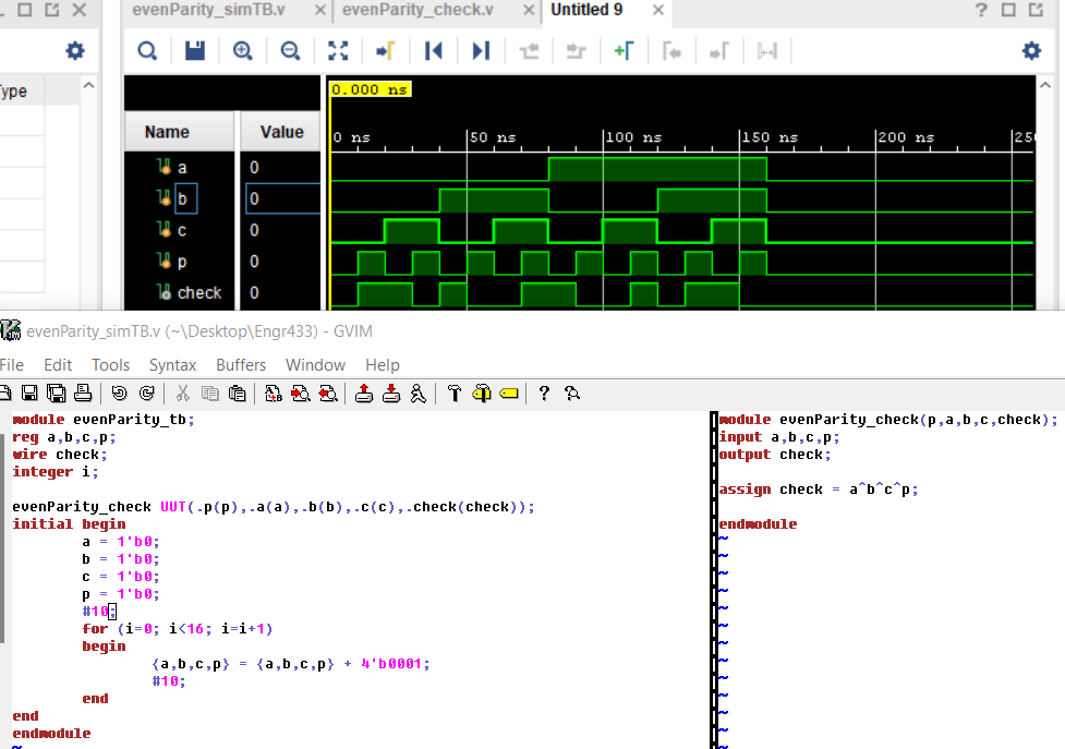
Figure 5. A screen snip of the Even Parity Checker behavioral simulation ran in Vivado along with the Verilog scripts
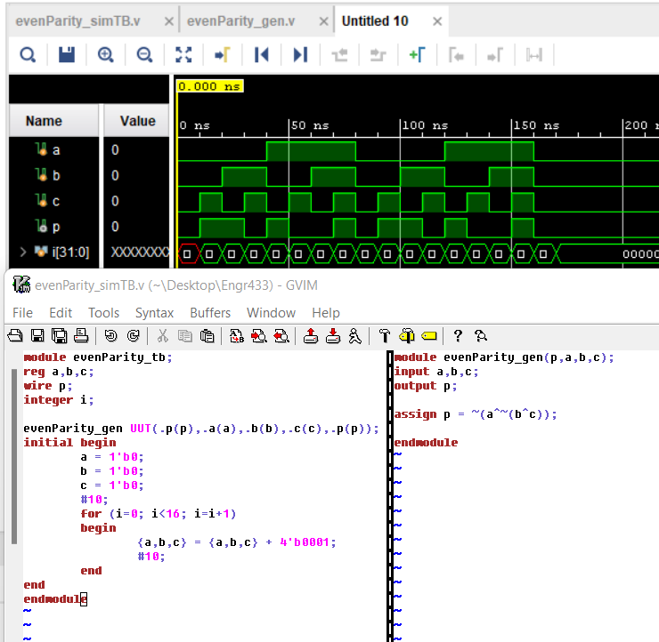
Figure 6. A screen-snip of the Even Parity Generator behavioral simulation ran in Vivado
used to run the simulation.
along with the Verilog scripts used to run the simulation.
Video 3. A recorded demonstration of the Even Parity Checker implemented on a FPGA.
Video 4. A recorded demonstration of the Even Parity Generator implemented on a FPGA.
Task 9
For the final task, improved versions of the home alarm and vacant parking-space counter from a previous homework were created and implemented on
a FPGA. A demonstration of the home alarm system can be seen in Video 4 below; a demonstration of the vacant parking-space counter can be seen
in Video 5 below.
Video 4. A recorded demonstration of the improved home alarm system on a FPGA.
Video 5. A recorded demonstration of the vacant parking-space counter being implemented on a FPGA.