Tutorial 4: Layout the padframe
There are two versions of padframes. The one with ESD protections is
the first one (new), it is more professional but I do not have a
webpage-based tutorial yet. The tutorial videos are available. The one
without ESD protections is the second one (old). You chip will work
fine by using the second one but it just looks bad and the chip will be more susceptible to
electric shocks.
2. A padframe without ESD protection: (old) (part of the following contents are from www.cmosedu.com)
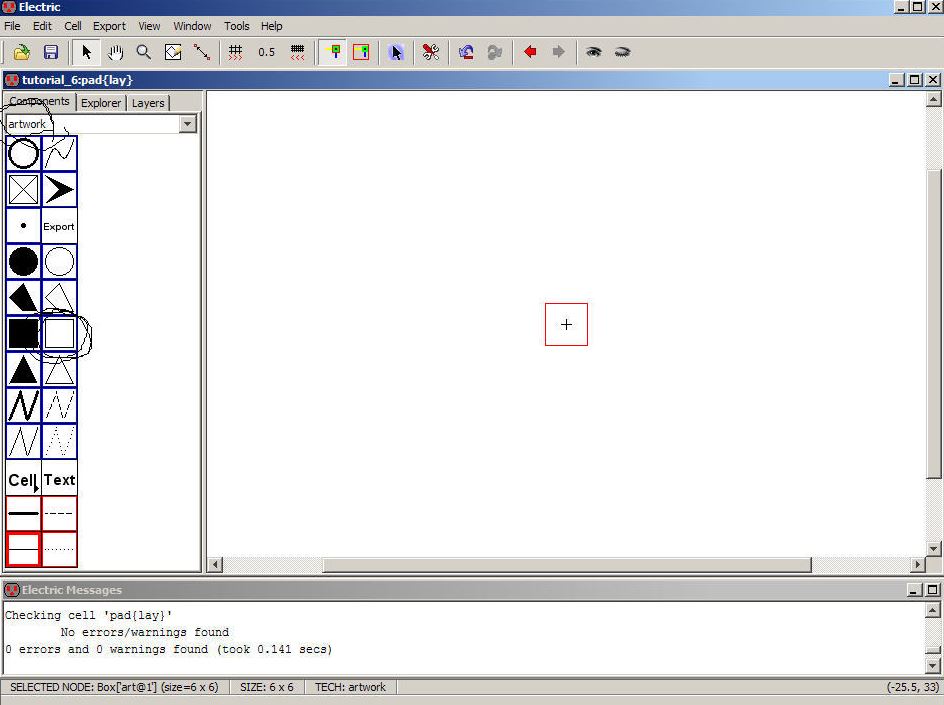
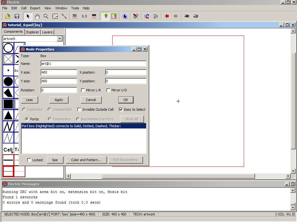
Create the layout view of a cell called “pad.” Go to the artwork menu and select/place a Box as seen below.
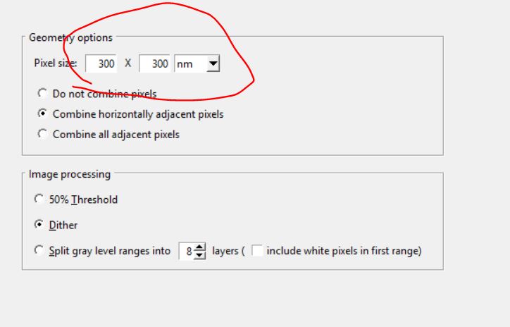
We
need to determine the size of the Pad cell above. The scale factor
(lambda) used in these setups is 300 nm so a layout that measure 5000
by 5000 is 1500 um by 1500 um (1.5 mm = 1500 um) If we have 12 cells on
a side (10 plus two corners) then each cell must be 5000/12 or 416.66.
We’ll round this down to 400 to ensure our chip is a little smaller
than the maximum size of 1.5 mm square. Change the size of the Box
above to 400 square and center it on 0,0 as seen below.
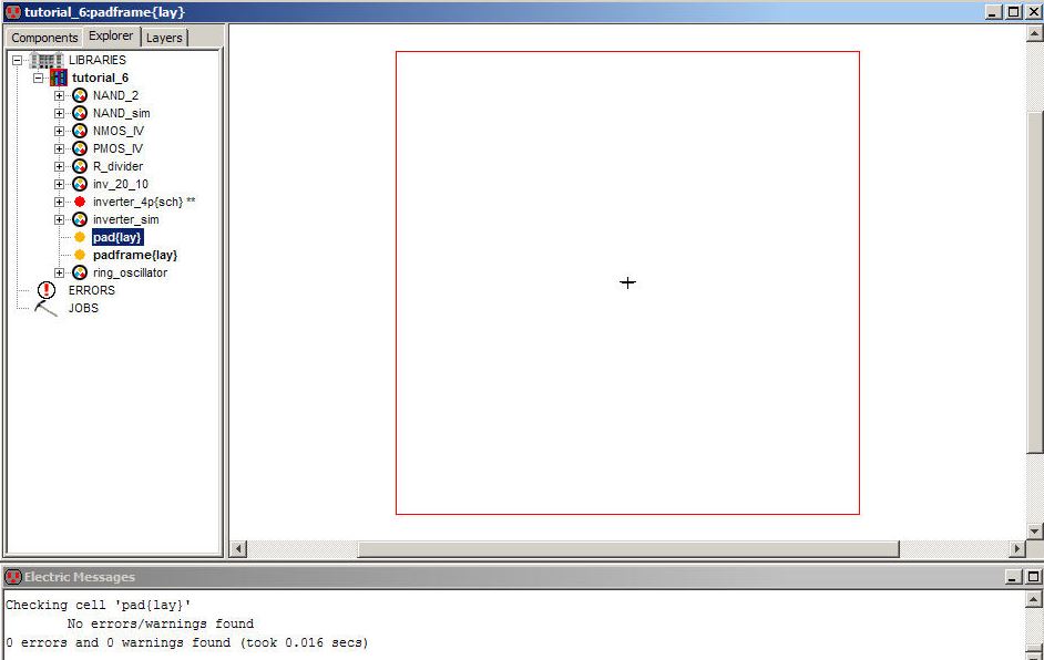
Before
we add anything to our pad cell let’s create a layout view of a
padframe cell (do this now). Place the pad cell into this padframe cell
as seen below.
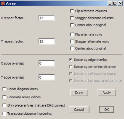
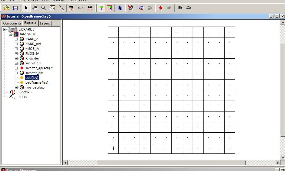
Next let’s use the Array command (Edit -> Array or simply F6) with the pad cell selected.
After filling the window we get the following.
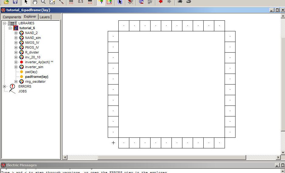
Next delete the corner and interior pad cells.
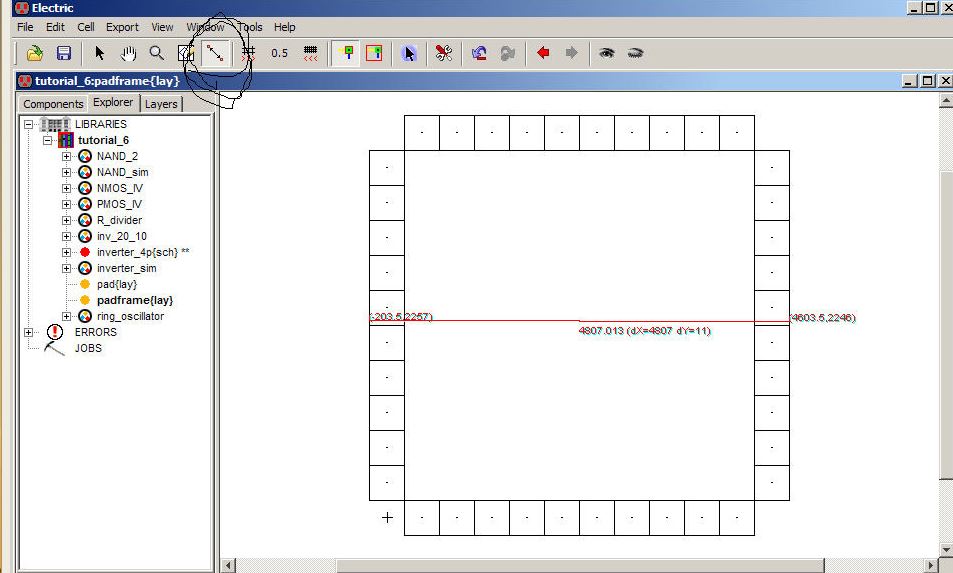
Let’s
measure the size of the cell using Windows -> Measurement ->
Toggle Measurement Mode (or press M or use the circled icon seen below)
Pressing M toggles back and forth between making measurements and the
normal click/zoom/wire cursor. Pressing Esc (or Windows ->
Measurement -> Clear Measurements) while in the measurement mode
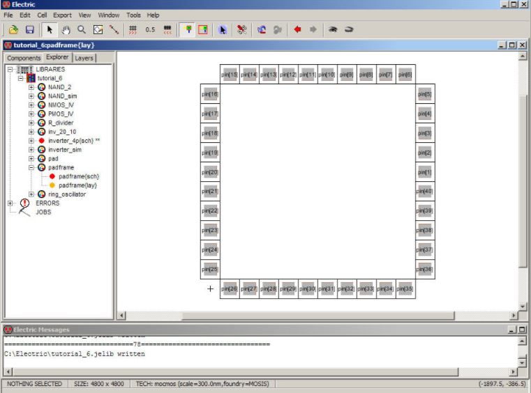
clears the measurements. Note that the exact size of the cell, 4800 by
4800, is seen at the bottom of the display.
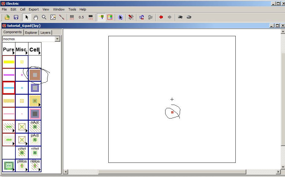
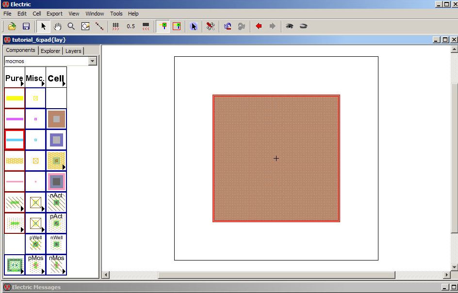
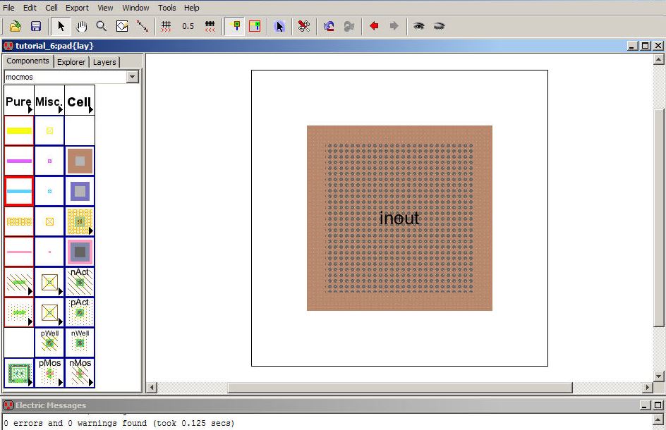
Let’s
go back to the pad cell and add metal to make the pad. We’ll using 75
um square bonding pads so, since the scale factor is 300 nm, a 250
lambda square piece of metal is used. Add a metal2-metal3 contact Node
to the pad layout as seen below.
Change the size of this Node to 250 by 250 and center it on 0,0 as seen below.
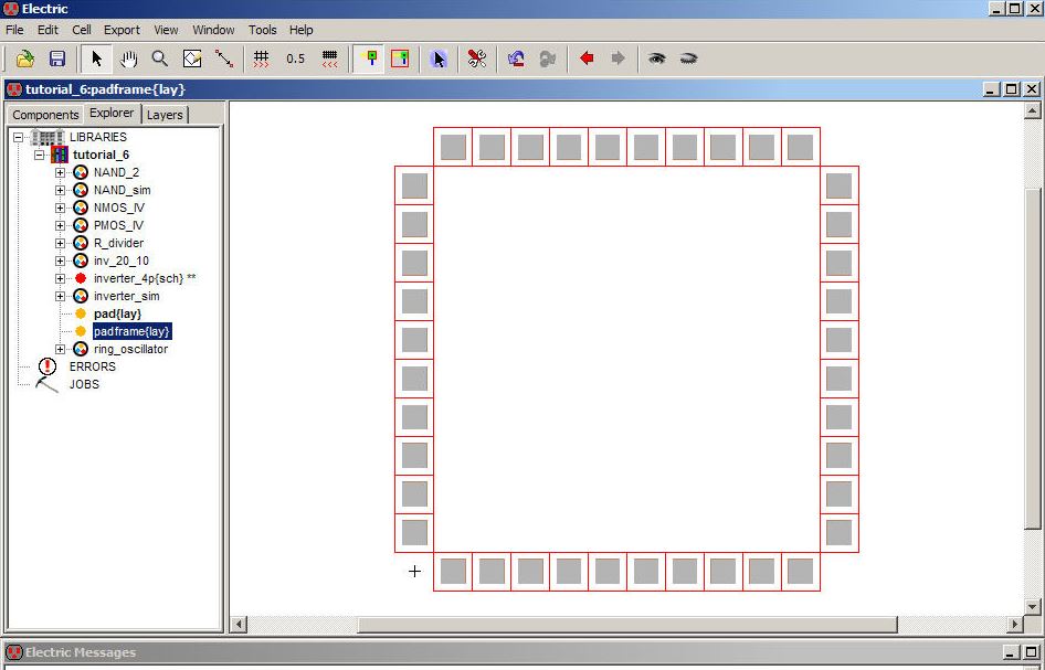
Our
padframe now looks like the following (after selecting the cells and
using the open-eye on the menu to show the cells’ contents).
Let’s
go back to the pad cell. We need to do two things to this cell, add an
Export so that we can connect to it, and add the Passivation layer
(sometimes called overglass) so that the top layer of passivation
(glass) is removed and get access to the metal3 (else we can’t get the
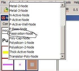
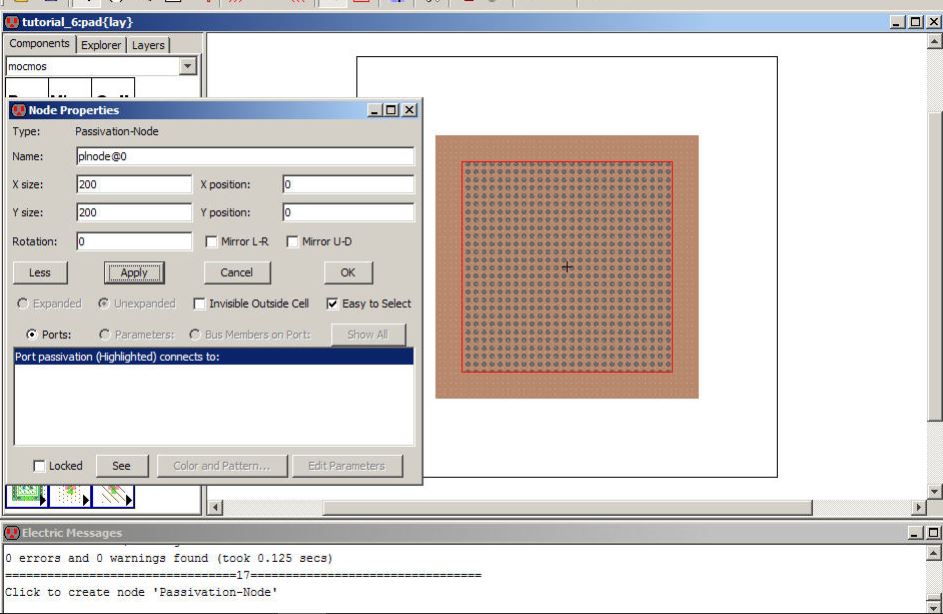
signals off chip!). According to the design rules the minimum overglass
opening is 60 microns (200 with our 300 nm scale factor). Add a Pure
layer of Passivation to the pad cell.
Next change the size of this Pure-Node to 200 by 200 and center it on 0,0 as seen below.
Next
select the metal3-metal2 Node and Export it as inout. Change the size
of the Export text to 25 as seen below. DRC your design to ensure no
errors.
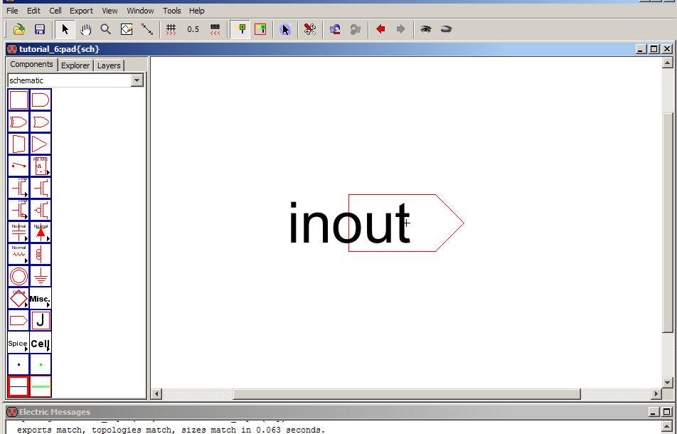
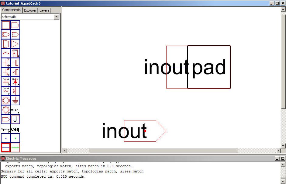
The
layout of our pad is complete. Let’s now make a schematic
representation for this layout. Create a schematic view of the pad
cell. Add the off-page Node and Export inout as seen below. Check the
schematic (F5) and NCC the layout and schematic views.
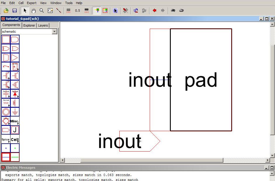
Next, go to View -> Make Icon View
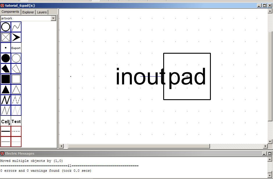
Descend
into the icon. Select the box and use Edit -> Modes -> Edit ->
Toggle Outline Edit (or just press Y) to adjust the size of the box.
When finished adjusting the size press Y to get out of this mode.
Adjust the sizes until you get something that looks like the following.
The schematic view of the pad now looks like the following.
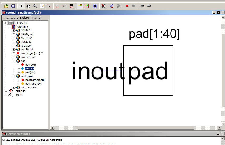
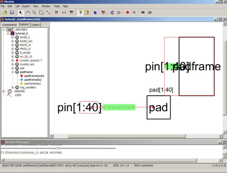
Let’s
create a schematic view for the padframe (do this now). Place the icon
of the pad into the schematic view of the padframe cell and change its
name to pad[1:40] (and move the name) as seen below.
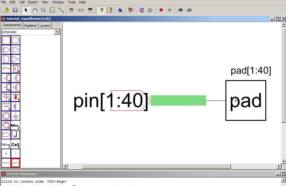
Next
add an off-page Node and connect a bus between the pad icon and the
off-page Node. Export the port of the off-page node as seen below using
the name pin[1:40]. The thick green wire represents a 'bus' whcih has
40 wires in the bundle. When you connect the pin to the pad, click the
green wire at the left bottom conor of the menu, then select the pin,
then connect to the pad by a right click at the terminal of the pad.
You must use the bundle to make a padframe schematic in this
experiment.
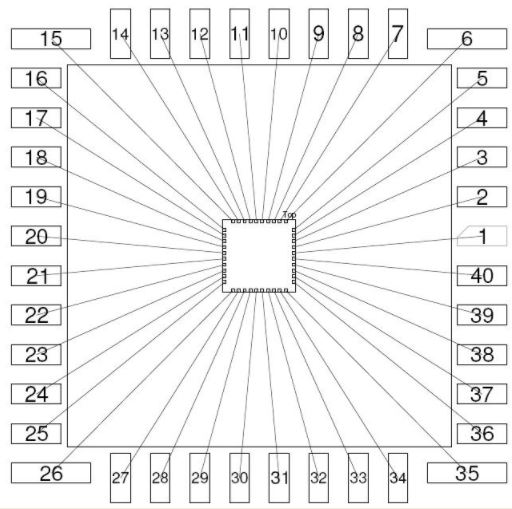
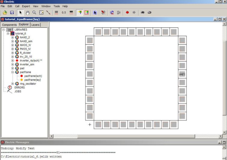
We
haven’t exported anything in the padframe layout so we need to go back
and do that. However, it would be nice if pin[1] corresponds to pin1 of
the package. MOSIS uses a 40 pin DIP package for the educational
program with a bonding diagram seen below (our padframe, that is, chip
is in the middle of the figure).
Pin1
of the package is connected to the fifth pad from the top and the right
side. Let’s export this pin on the padframe layout now (and change the
export text size to 125).
We
need to do this for the other pins. One trick, after you’ve exported
all the pins is to select the entire layout, then Ctrl+I it and
removing everything but the text. Then change the text unit size to 125.
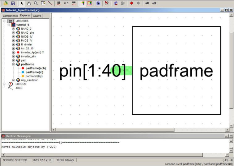
Next let’s create an icon view for the padframe. Go back to the schematic of the padframe and use View -> Make Icon View
Descend
into the icon view of the padframe and use Edit -> Modes -> Edit
-> Toggle Outline Edit (or just press Y) again to adjust the size of
the box. Move the Export text to the left until you get something that
looks like the following.
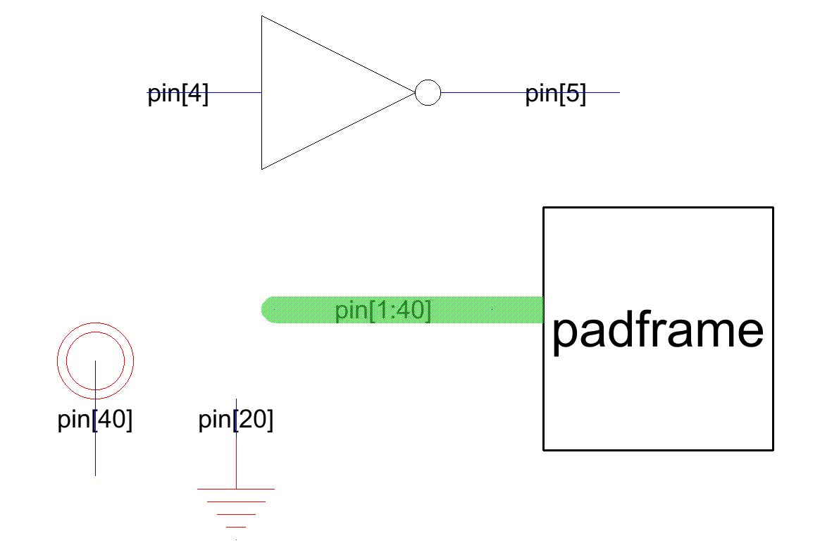
Now, Create a new cell, start with a schematic named 'Chip'.
Drag
the inverter icon you designed in the previous lab to this schematic (Chip),
also drag a 'vdd' and a 'gnd' to the schematic. Extend the 'bus bundle'
from the 'padfram' and 'ctrl+I' the arc (notice, the arc not the pin),
and name the arc to 'pin[1:40]'. Use the same way name the input
and output arc of the inverter to 'pin[4]' and 'pin[5]', name the vdd
and the gnd arc to 'pin[40]' and 'pin[20]'.
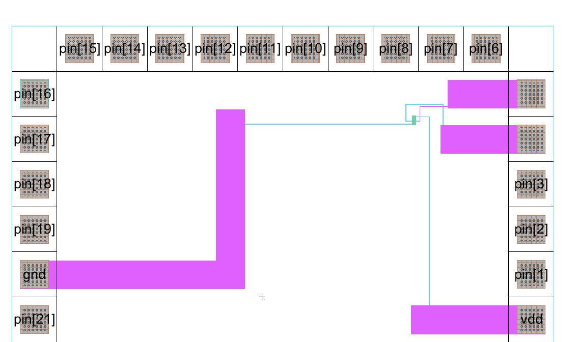
Go
to the layout view, connect vdd and the gnd of the inverter to pin[40]
and pin[20], connect input of the inverter to pin[4], the output to
pin[5]. Notice that the blue wires are Metal 1, the violet wires are
Metal 2, you must avoid any intersections of Metal 1 since they are in
the same layer and will cause shorted circuit. Use different layers of
metals to aviod the intersectinos.
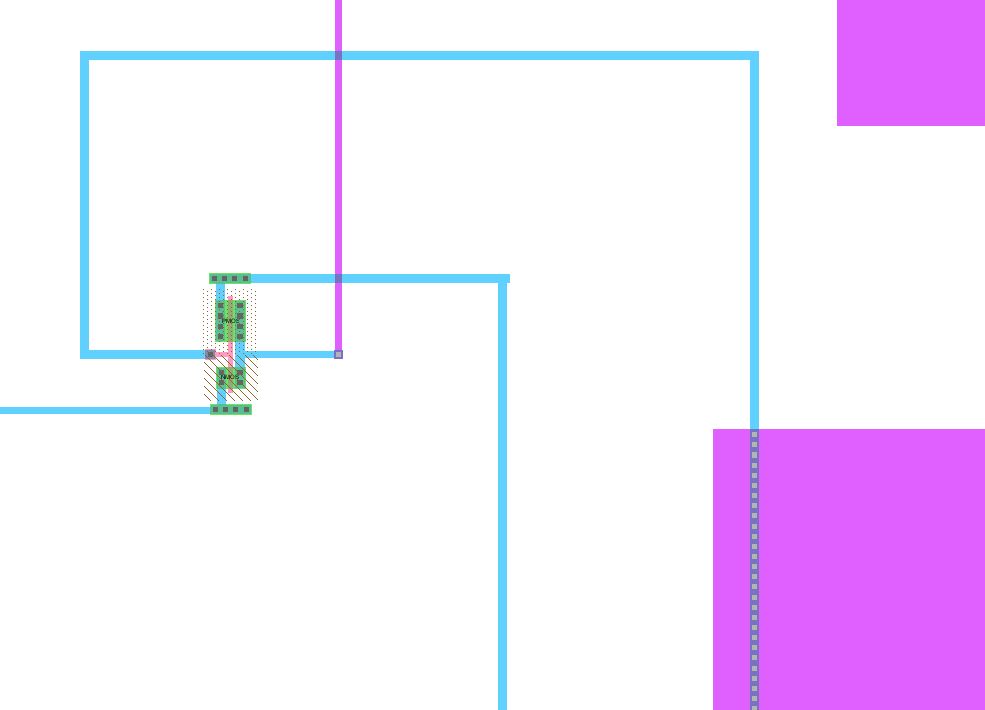
Zoom-in to the inverter.
When
you connect wires to the pads in the padframe, you must be careful. Try
to use 'ctrl + left click' to select a single object, use 'shift + left
click' to select two objects at the same time. In order to connect two
objects in the padframe, you must select the two objects and the
same time (use shift), then connecct them. Look at the figure below
which shows the 'vias' on the Metal 1 - Metal 2 overlapped area. This
is a valid connection. Otherwise, the two layers of metals are running
in parallel which doesn't have any connections. Zoom-in the connected
area to check if you have the 'vias' there.
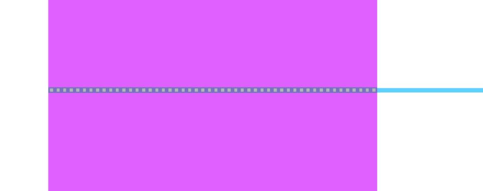
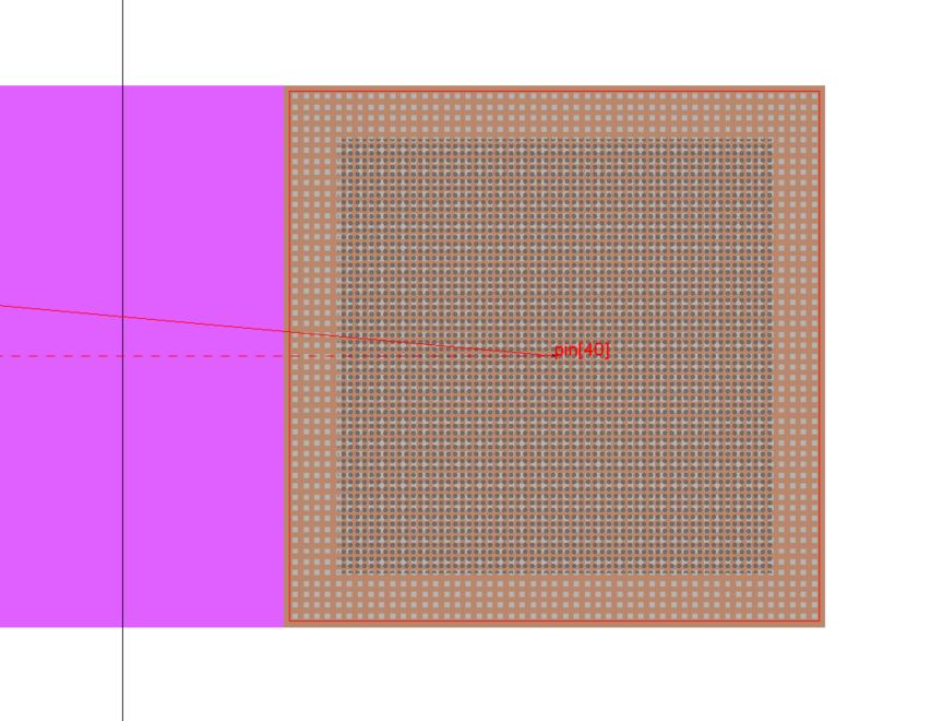
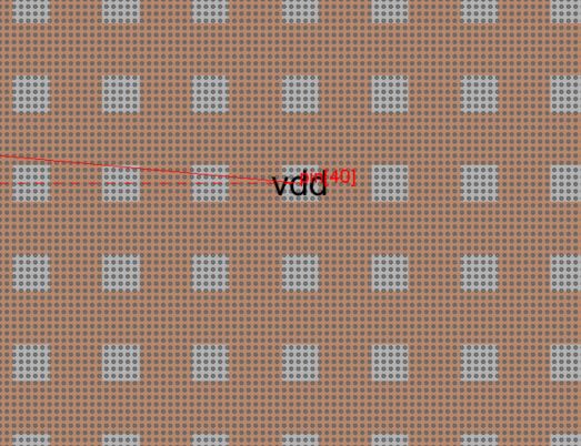
You
must export the vdd and the gnd pad. However, the initial fonts are
tiny (like the figure below), you can't see the name of the ports.
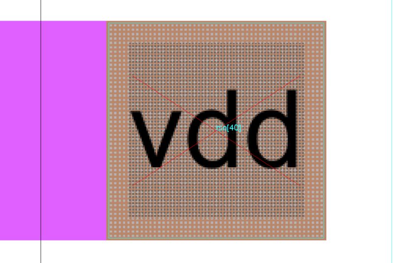
Zoom-in
to find out the location of the initial port name, and ctrl+click to
select the text, then change the font size to 125 units.
You should have the following font after the modification.
Then DRC, NCC, and ERC the schematic and the layout of the final chip.
Adding a logo to the chip is optional. If you are doing this lab for the ENGR 337, you do not have to do the following tasks.
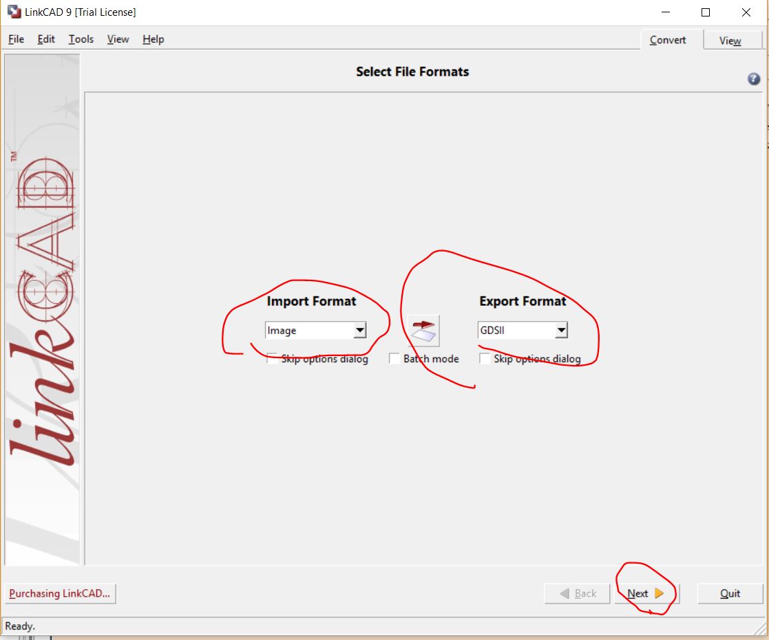
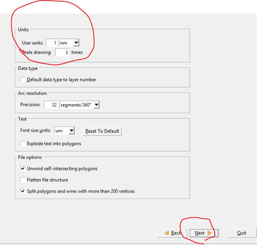
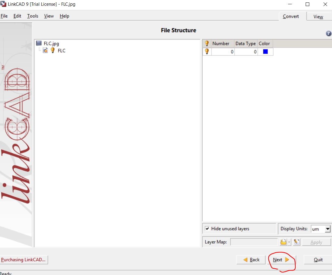
Now, let's add the FLC logo to the chip. Use 'LinkCAD' to convert a .jpg image to 'GDSII' format: Download the figure here.
Find LinkCAD in your C drive, program files.
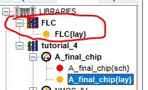
Then go to ELectric, File-Import-GDSII (stream), to load the .gds file you just created.
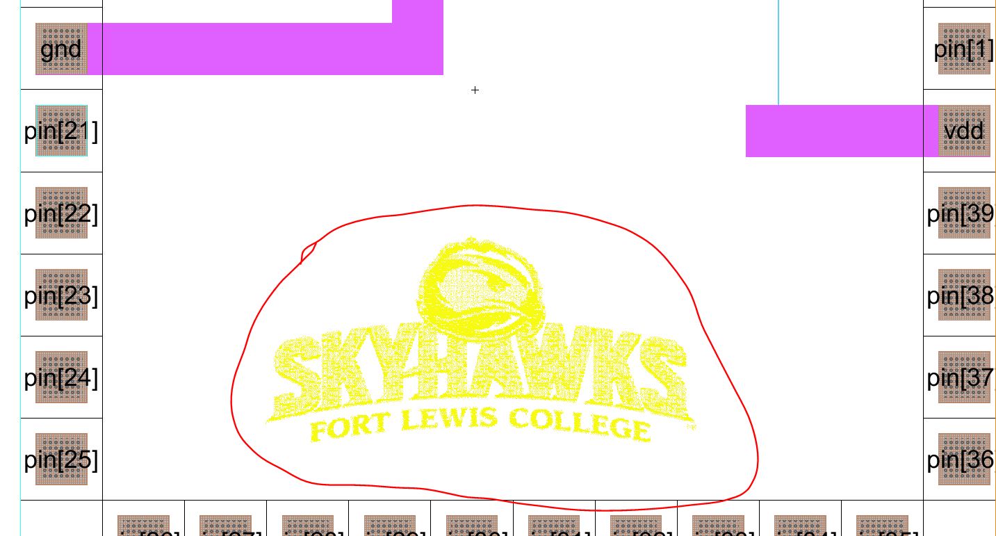
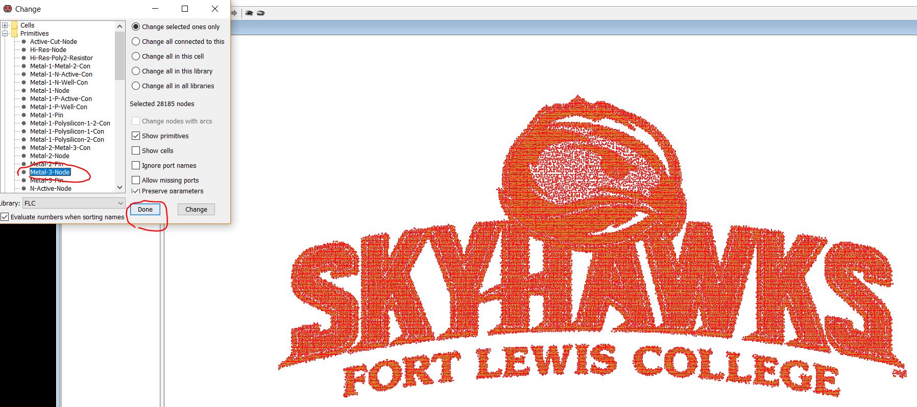
Go
to the FLC layout view, ctrl + A to highlight all pixels, then press
'c' on your keyboard, change the layer of the pixels to Metal 3 node.
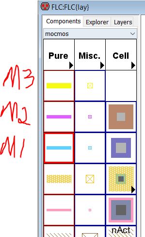
The cloor of the metal layers are:
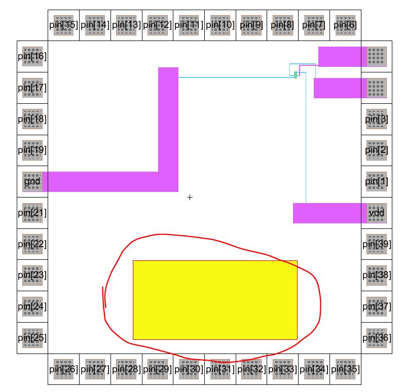
The final view looks like the following: Zoom-in to see the details of the logo.