The Preamplifier PCB Design for the Oximeter Circuit
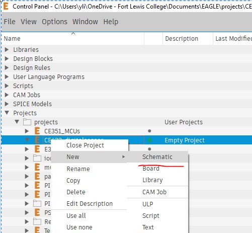
Start a new project.

I named it CE433_digitalsensor

Right click to create a new schematic.
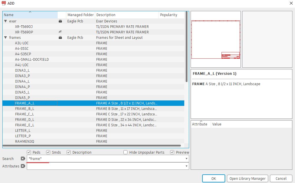
First add a frame to your schematic and give a title to it.

Make
sure that you enable all the libraries such as the Sparkfun library and
Eagle's library. Follow my Eagle PCB tuturial to load the Sparkfun
library and enable it.
Search for an amplifier that has the same SOT-235 footprint.

You
must create a new library for this type of component. If you expect to
have multiple ampifiers in the future, you can just name it as
myAmplifier.
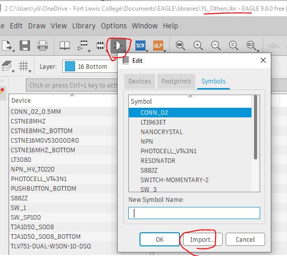
Get into the myAmplifier library, create a new device by importing the one we found above. (the OPA amplifier).
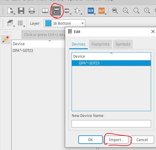
Search *opa658n*, it should show up in the window, if it doesn't, please check if the Eagle Pcb library is activated or used.

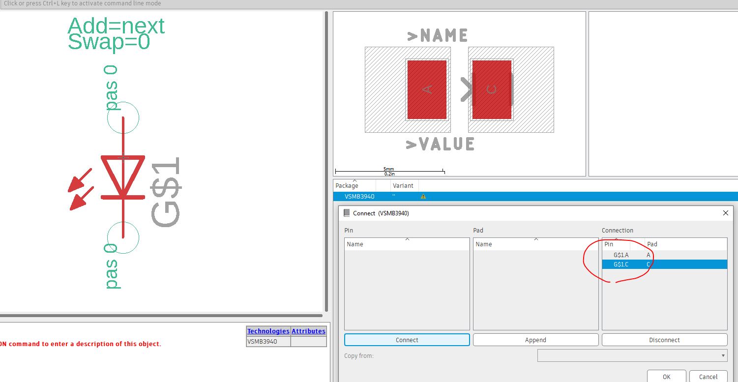
Check the pinout of the LT6003 OpAmp to see if it matches the OPA amplifier's pinout.
It is Out, V-, IN+, IN-, and V+ from pin 1 - 5.
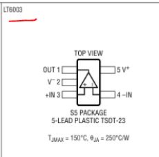
It machtes the schematic symbol.
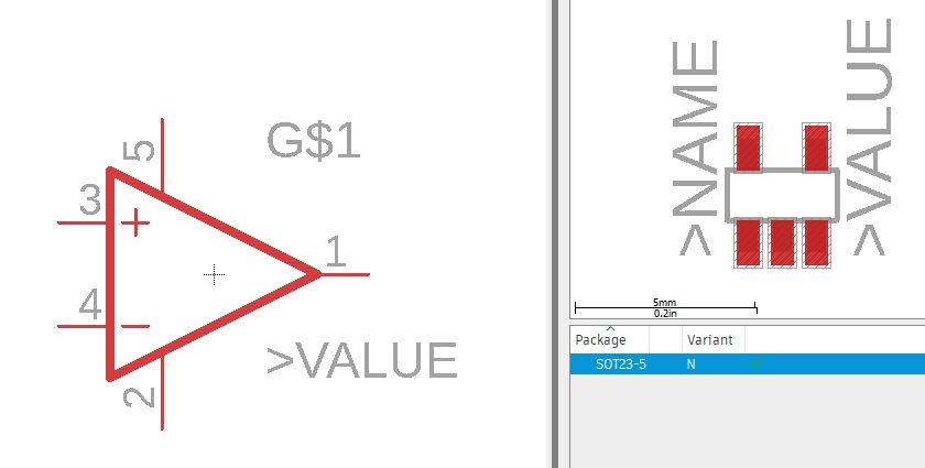
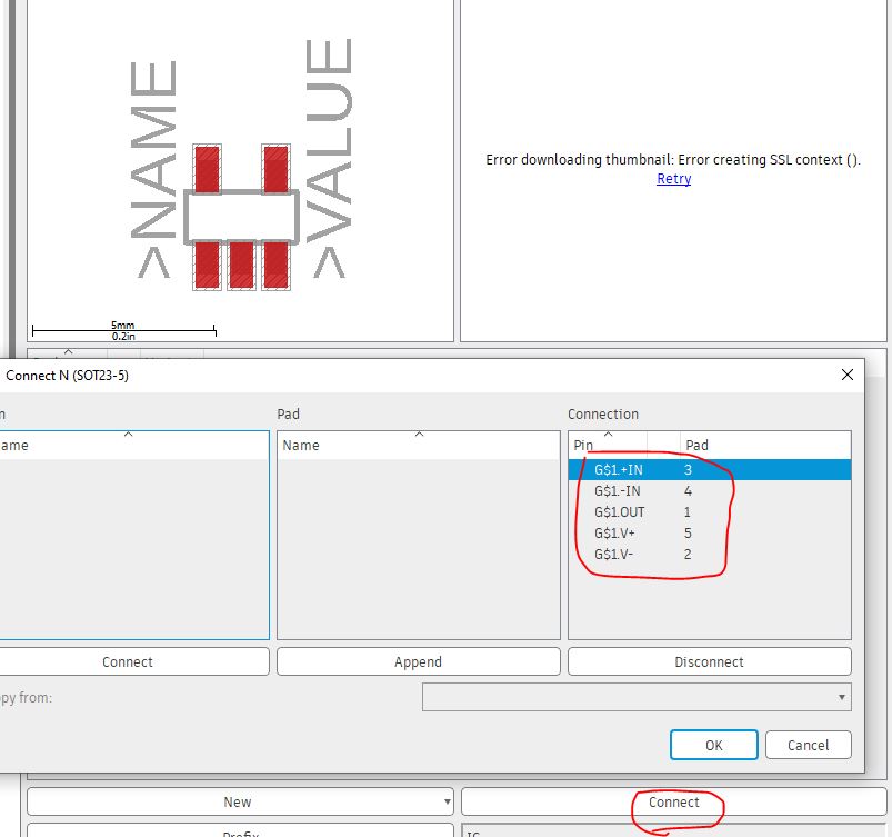
Click 'connect' and you can find that the pinout of the symbol and the pinout of the layout match.
Save the library.
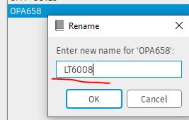
Rename the loaded OPA amplifier device to LT6008.
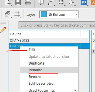
I mistyped it, it should be LT6003.
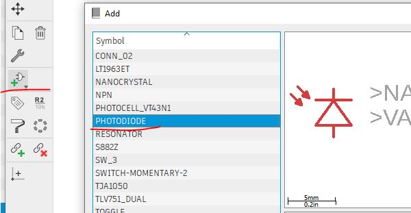
Then import a photodiode.
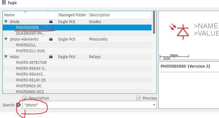
This symbol looks great, let's use it.
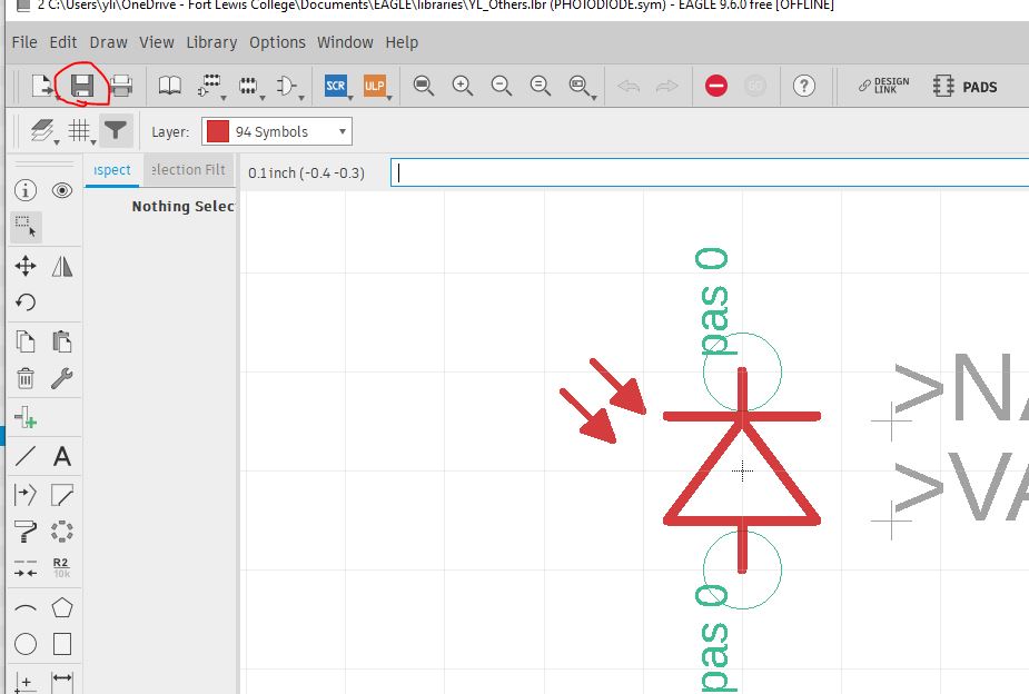
Save it.
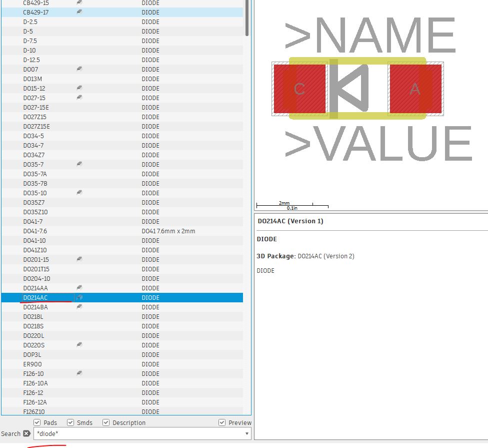
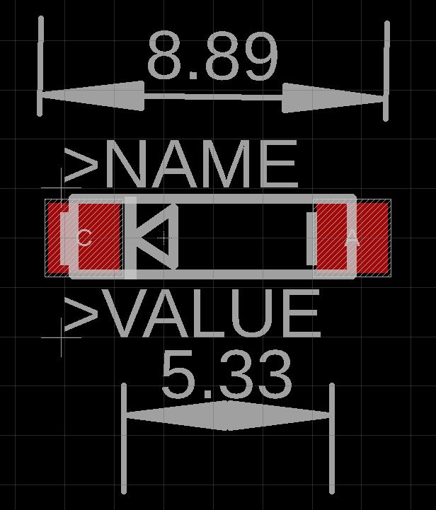
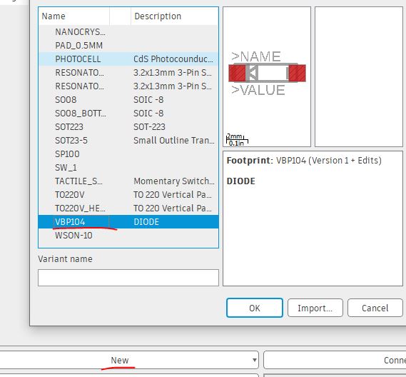
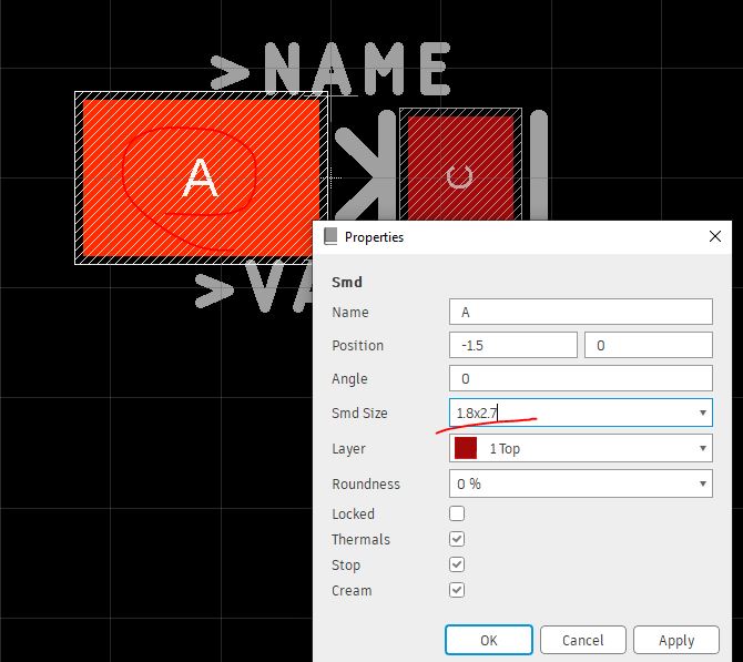
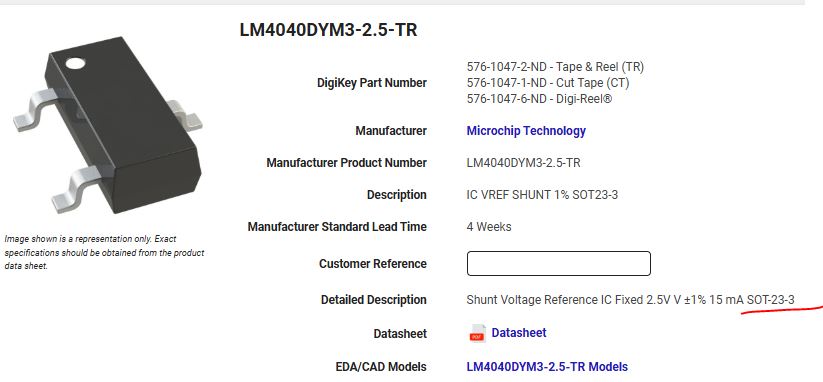
Find the footprint of the photodiode from the datasheet.
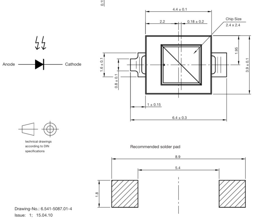
Follow
the recommended solder pad dimension. I imported a diode layout pad and
modified it to match the dimension in the datasheet.
Here is the diode layout I imported to start with.
Stretch the edgets to make it longer.

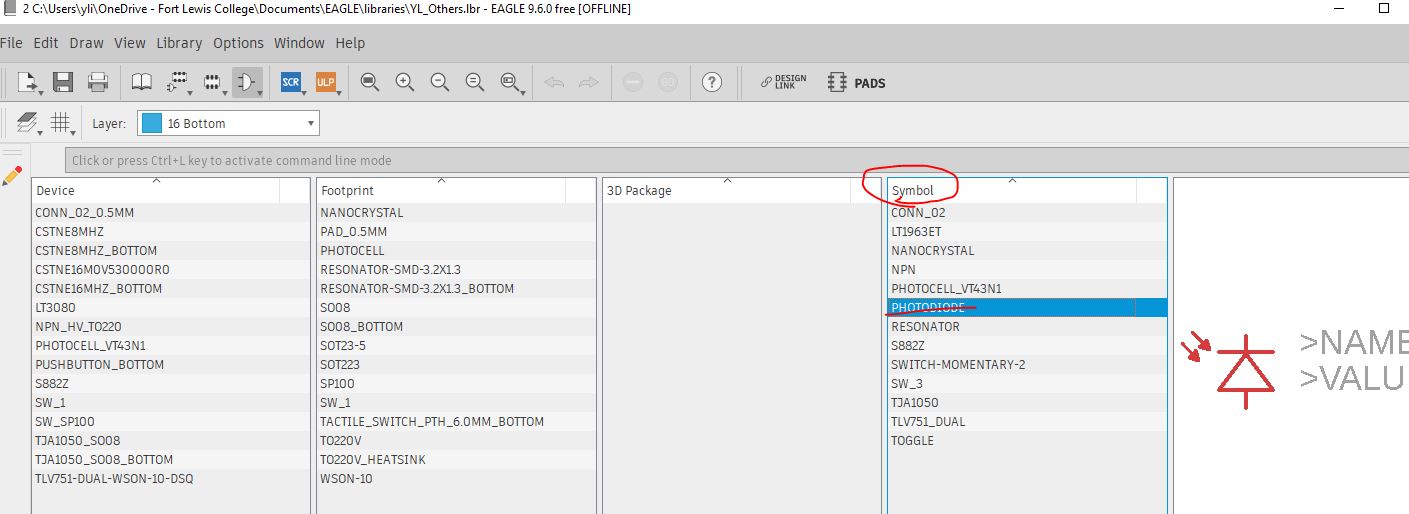
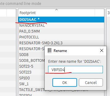
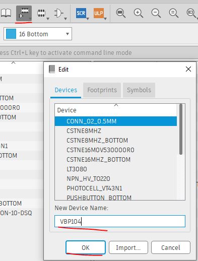
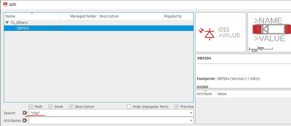
Rename the footprint to VBP104:
Create a new device called VBP104:
Getting into the device editing window.
Load the layout view as a local package.
Connect pins from schematic to the layout.
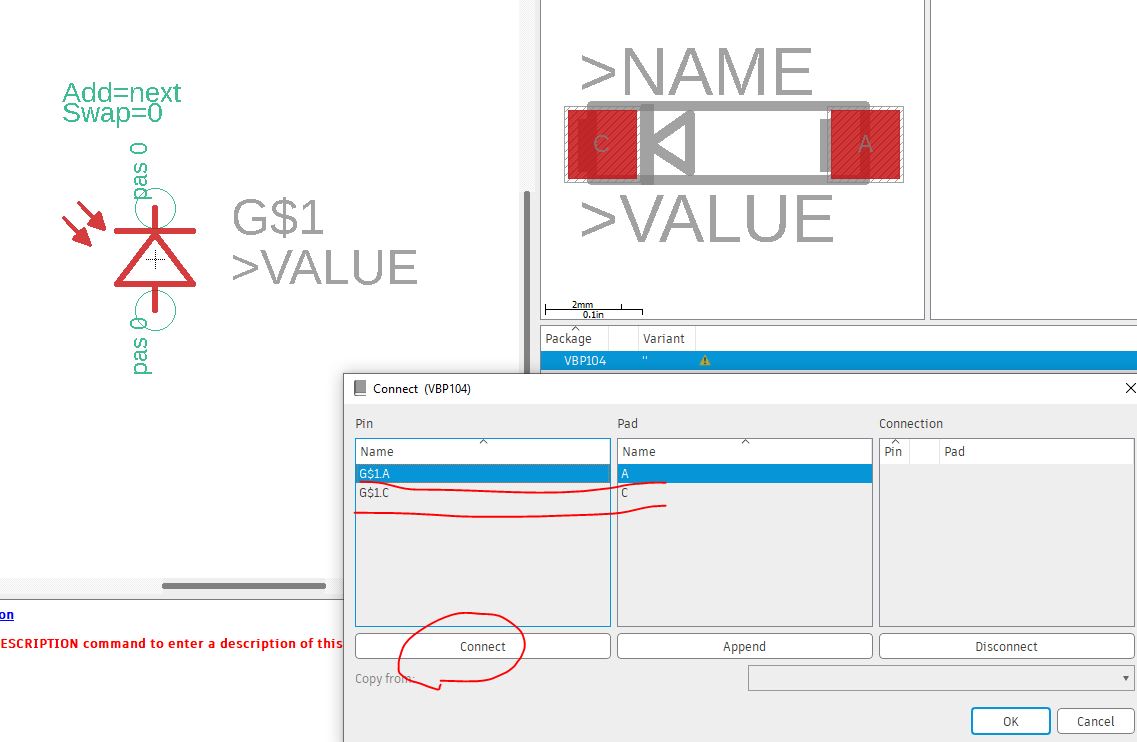
Save it.
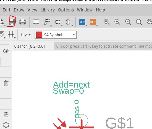
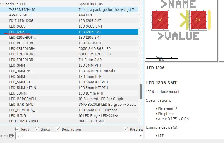
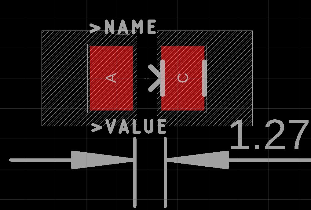
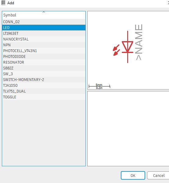
Add an LED device for the IR LED. The symbol could be a regular LED's symbol.
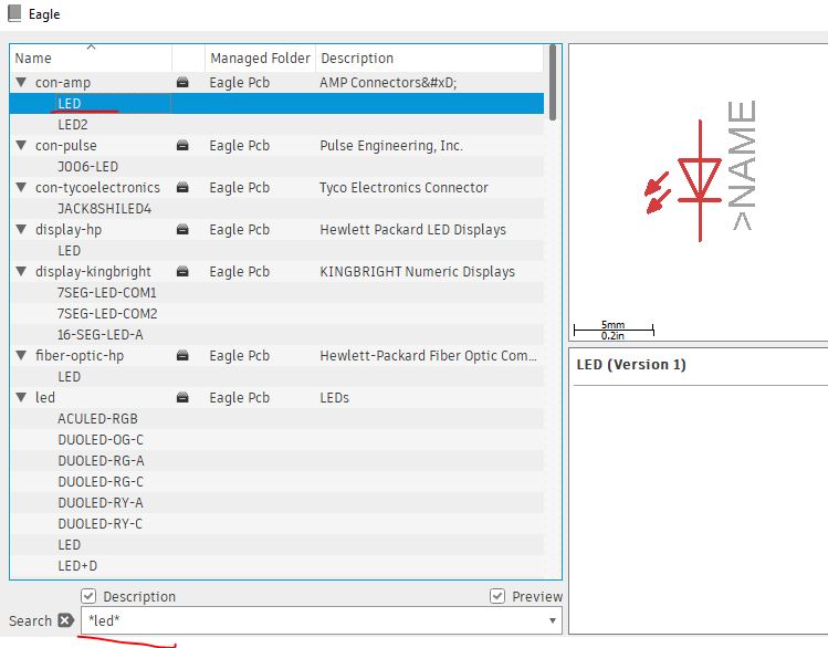
Find a LED 1206 pakcage. 1206 means 0.12 inches by 0.06 inches by size. This is a good size for soldering.
Find the footprint of the IR LED from the datasheet.
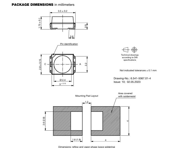
Modify the dimension of the layout accordinly.
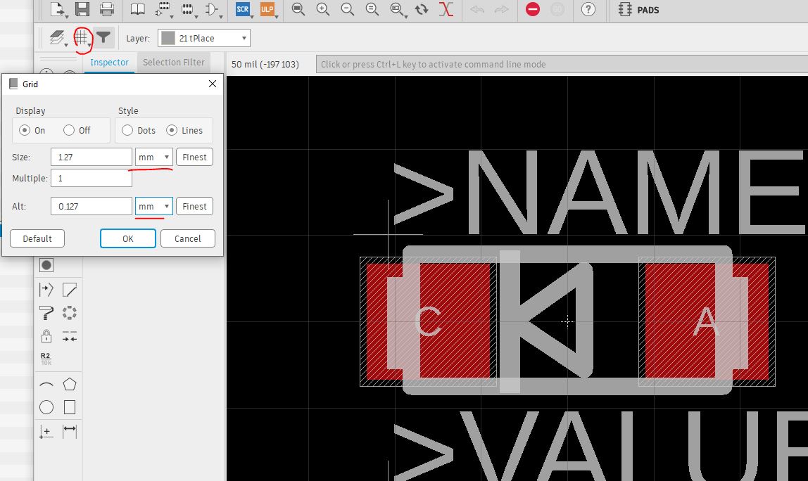
Draw rectangles using the tStop layer.
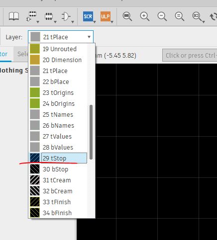
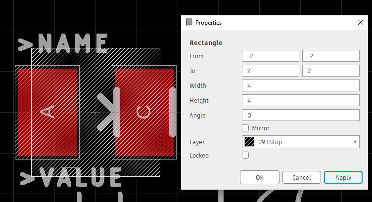
Move the tStop layer. The tStop layer keeps the area unpainted by the solder mask.
Edit the device by loading the schematic and the layout.
Make connections between the symbol and the layout.
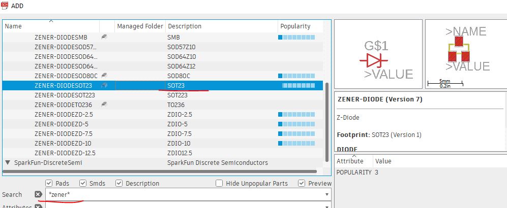
Now the zener diode.
There is a device in the library that can be used for the same purpose.
Open your schemtic, search for *vbp* to find the photodiode you just created.
Same to the OpAmp, add it to your schematic.
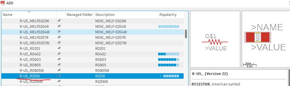
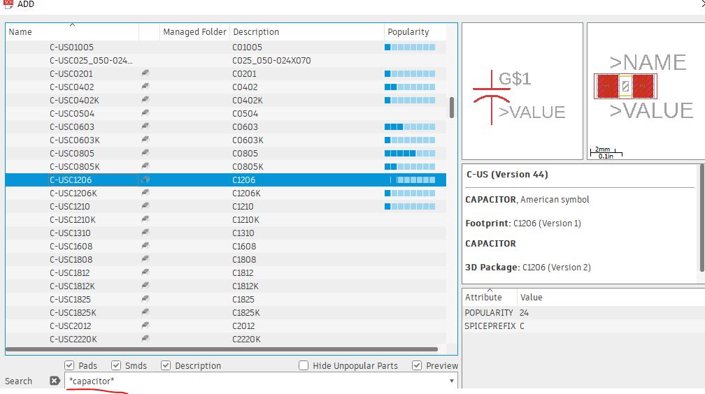
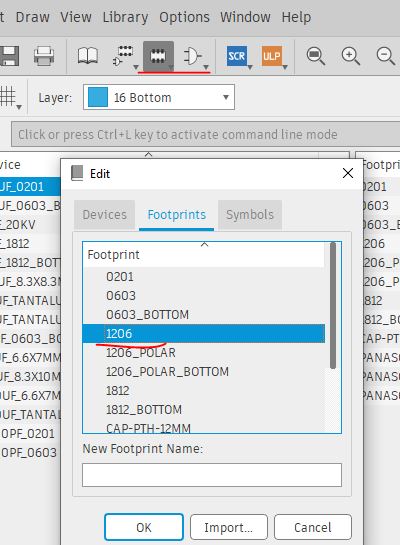
Add resistors and capacitors for the design. Make sure that they are 1206 footprint.
I didn't like the curved symbol for the capacitor since the capacitor we used is nonpolarized.
Let's created a 1206 capacitor with straight lines for the symbol.
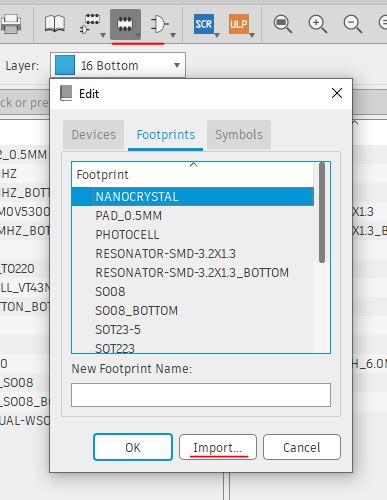
First, load the 1206 footprint.
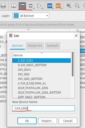
Create a new device
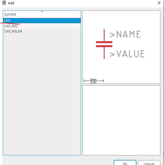
Import a schematic symbol.
Import a 1206 footprint.

Make connections between the symbol and the footprint to form a device.

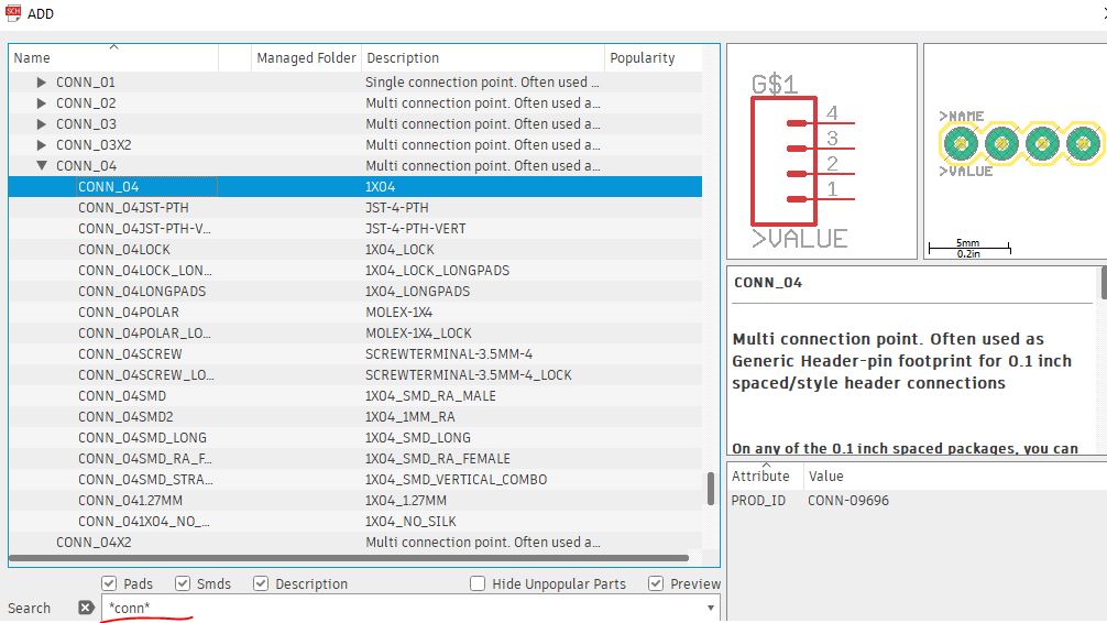
Add connectors. These will just be the standard hole on the PCB for header pins.
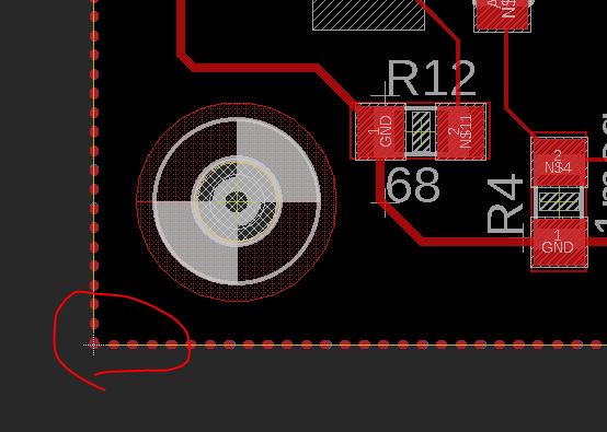
Add screw holes to the four corners of the board.

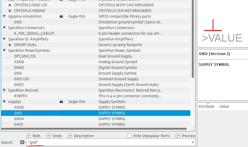
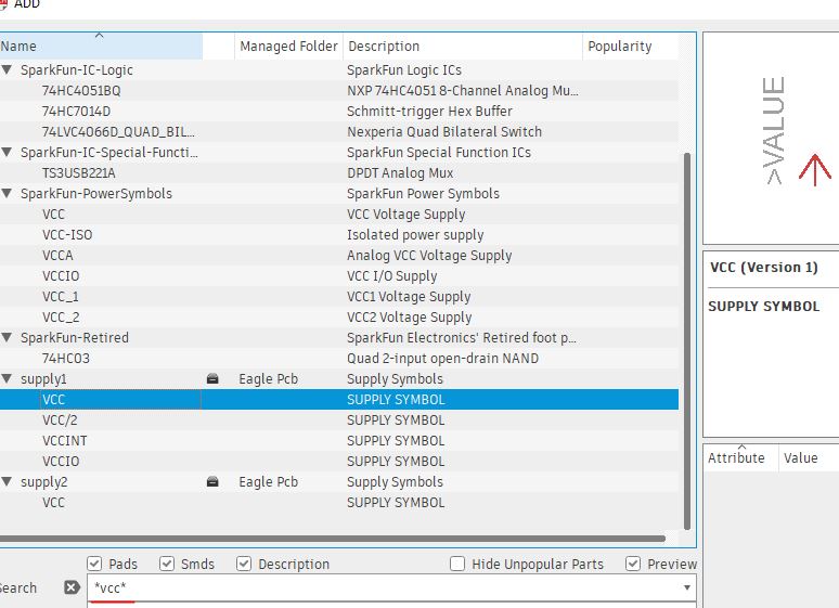
Add the GND and VCC symbol.
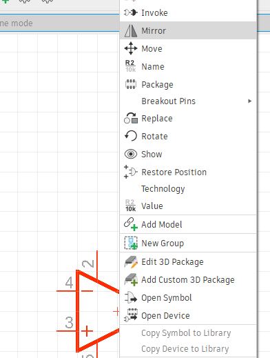
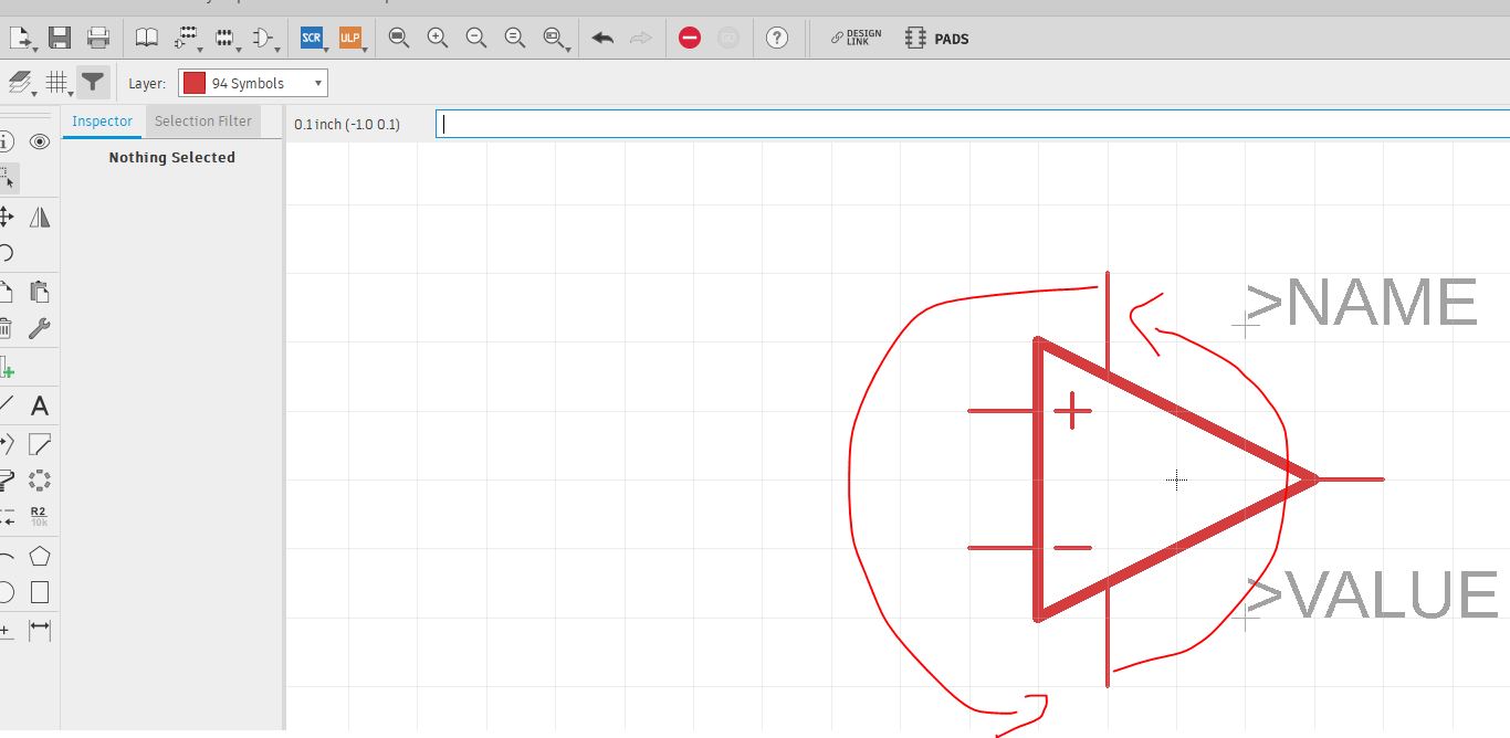
The OpAmp symbol doesn't have the desirable orientation. The V- is on the same side of the inverting input terminal.
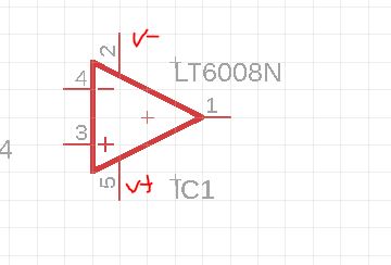
We have to get into the library and swap the VCC and GND pins.
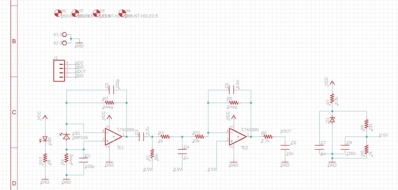
Place all the parts to the schematic view in the correct order and get ready for wiring.
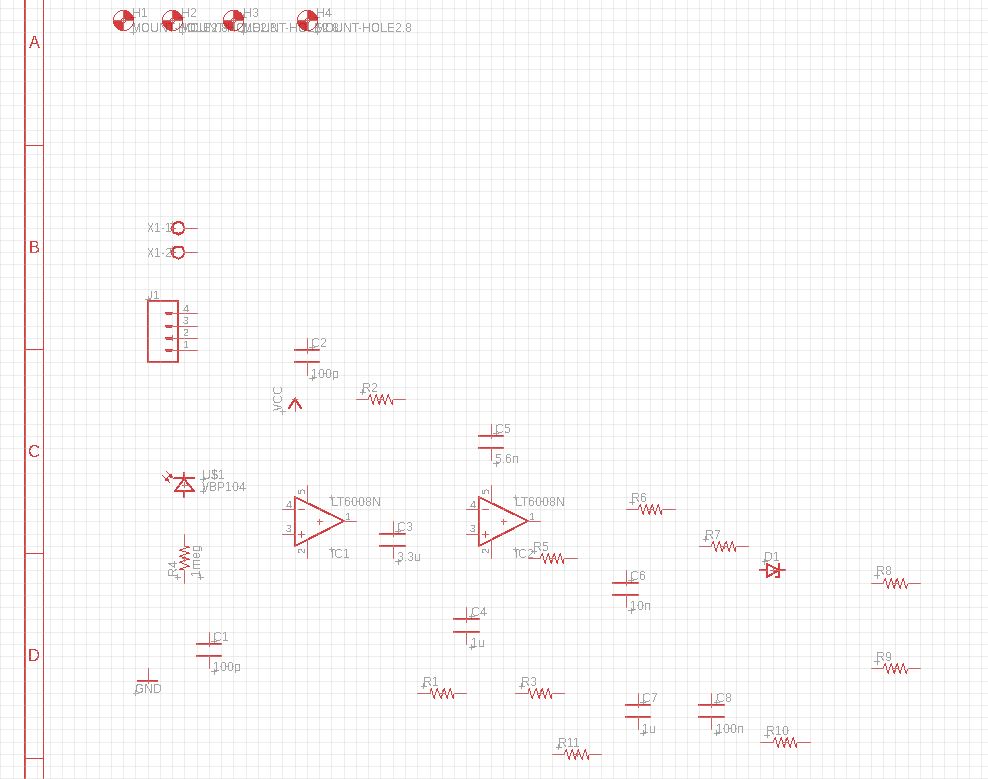
You
must right click and change the values of the resistors and capacitors
manually. Some of the capacitors don't allow you to do so. Use the ones
I recommned at the beginning of the tutorial will allow you to change
values of the parts.
Follow this tutorial to load a bmp image to your board. Here is the original FLC logo I found online.
Use this website to convert your image into black/white first.
Then use this website to convert the black/white (binary) image into a bmp file.
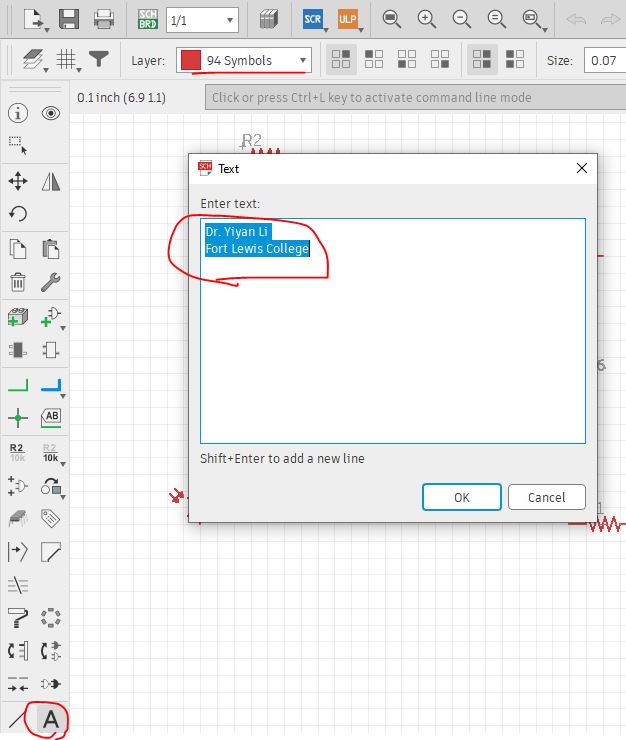
Also write a text on Layer 21 tPlace for the version number of the board.
Place
the parts in a certain order that helps your manual routing. Manually
route it first, only leave the tangled wire for the autorouter.
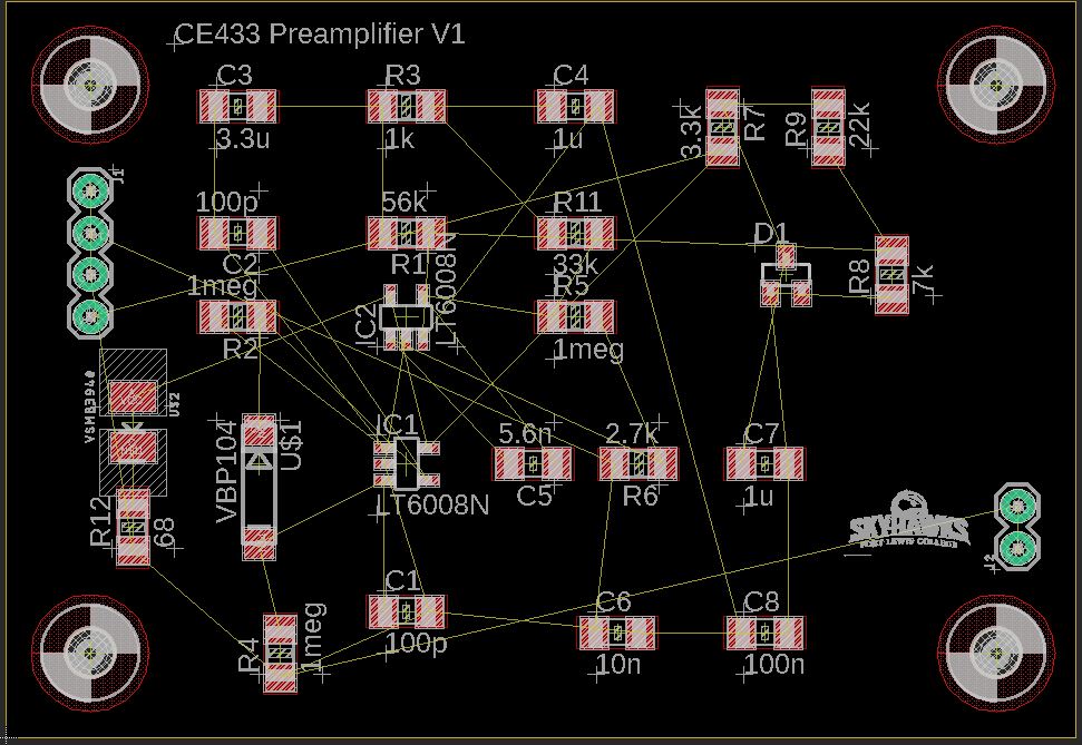
I Manuually route it to whatever I can, then I autoroute it afterwards.
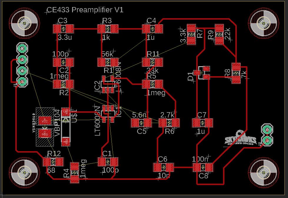
Then
auto route. Autorouter add a bunch of vias and traces at the bottom
layer. You can tell that it tries to save the space so they are very
close to some of the components. However these are allowed clearance by
the design rules so they are fine. Just be careful when you do the
soldering.
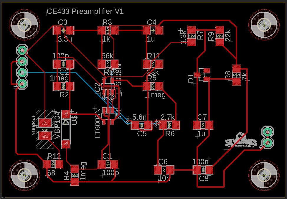
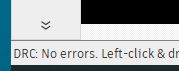
Make sure go through Tools - DRC check and it's error free.
Add a polygon to the demension, name the top polygon 'VCC" and the bottom polygon 'GND'.
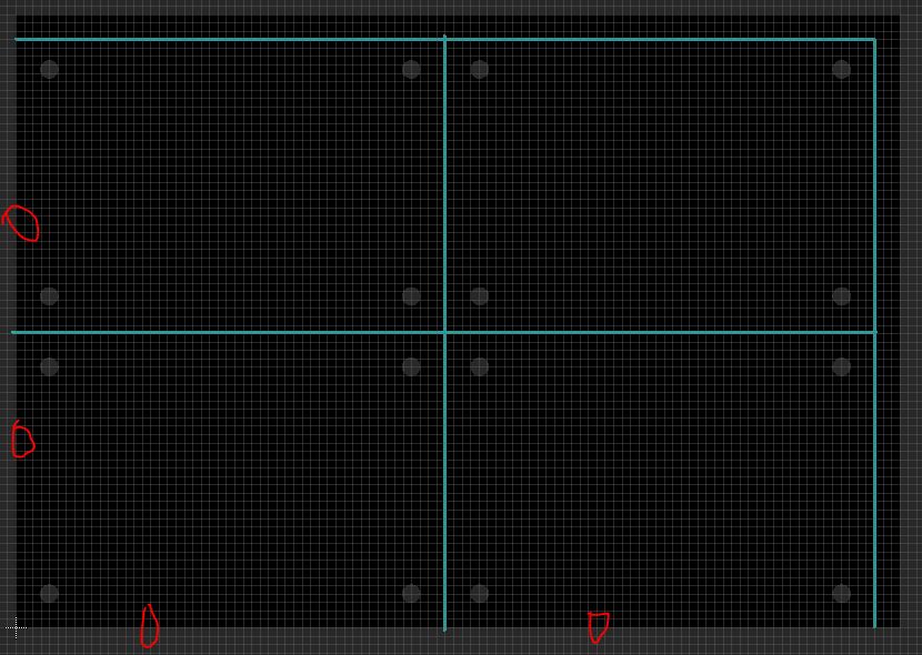
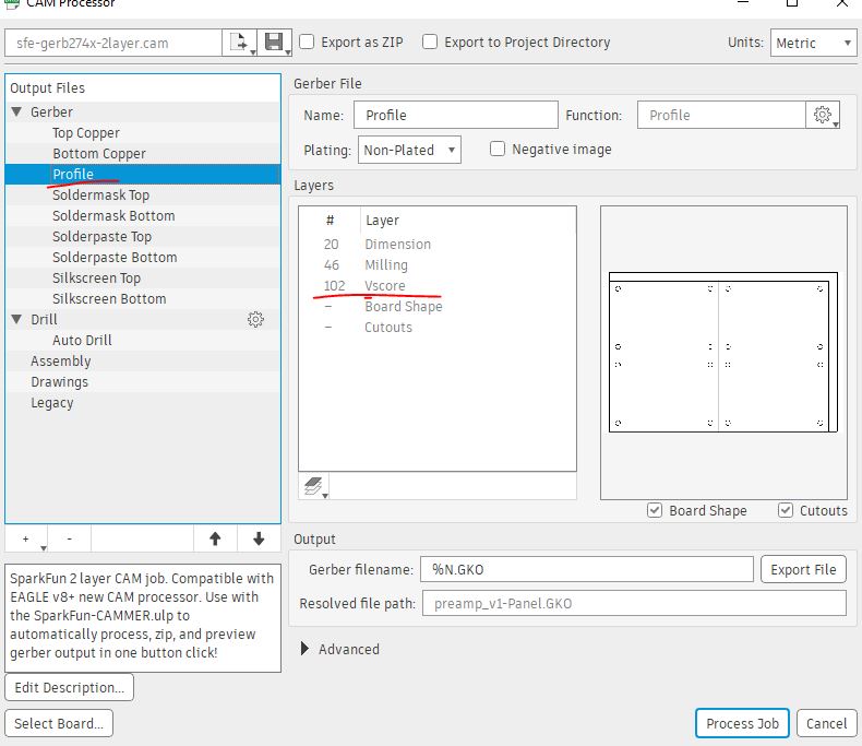
Follow this tutorial on how to penalize your PCB.

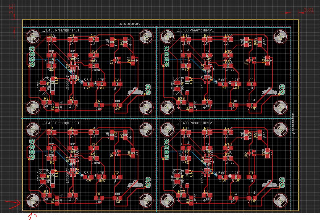
Only show the V-Score, you
should have the following view. Make sure that no V-Score on the marked
three edges. There will be a dimension layer defining these edges.
Follow the penalization tutorial to export the gerber files.
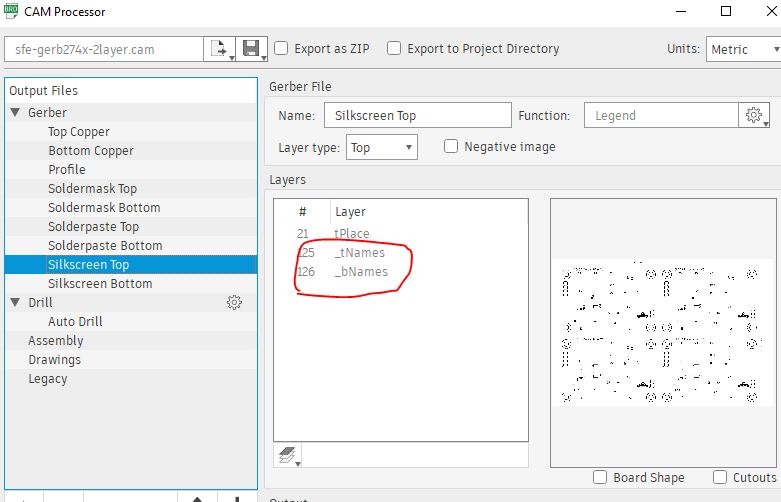
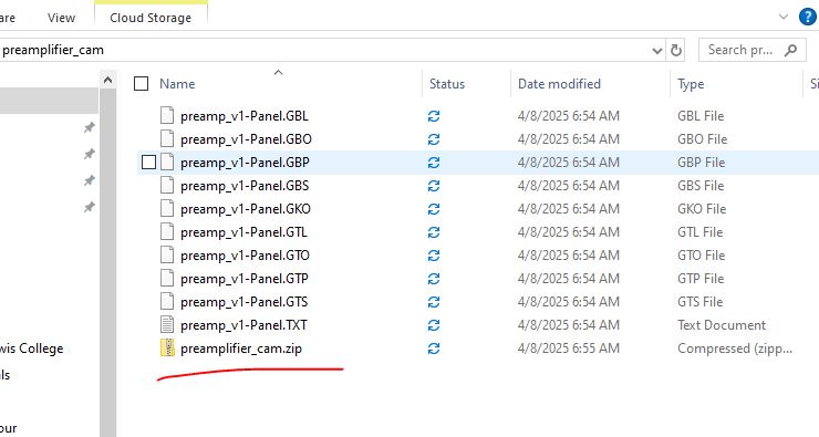
Upload it to JLCPCB for fab.