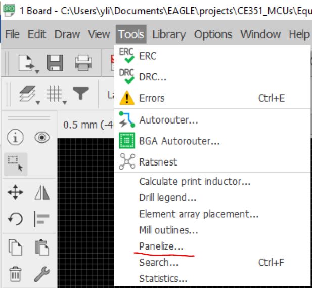
Panelize a small PCB layout design for lower cost
When the layout is completed, in the layout view, click Tools - Panelize
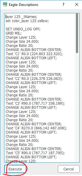
This process will identify board and parts numbers and standardize them
to prevent incremental labeling. For instance, when copying and pasting
a board layout in the same view, a resistor labeled R1 on one board may
become R52 on another board, depending on the number of resistors
present. Treating the incremented part number or name as a distinct
design may result in a significantly higher fabrication fee. If the
board got panelized, the same resistor on these replicates will show
the same numbers/names (all R1s, etc).
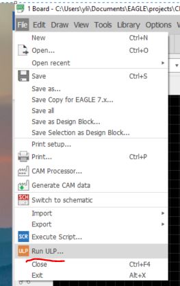
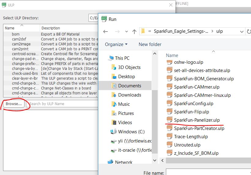
Download this SparkFun Zip folder and find the SparkFun-Panelizer.ulp script to run the panelizing process to put things in an array.
The JLC PCB standard size (without extra charges) is 10mm x 10mm. Keep
the size of the PCB smaller than this dimension will reduce the cost of
the fab.
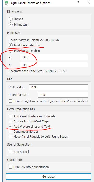
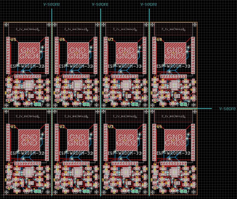
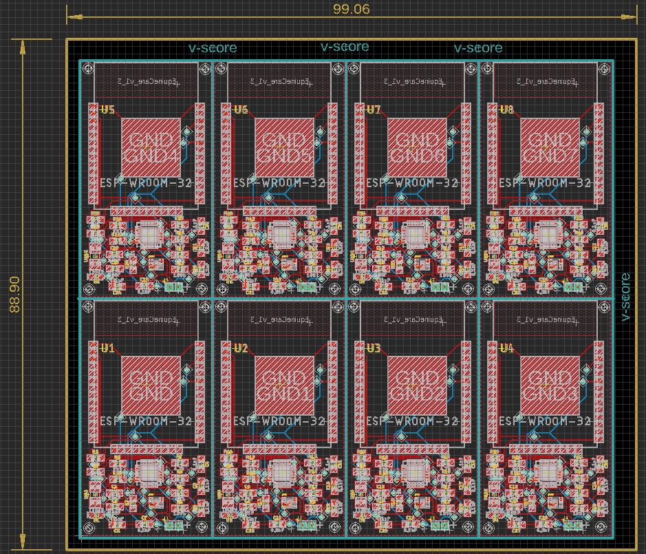
After clicking 'Generate', it will generate the following layout with the V-Score lines.
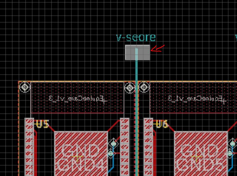
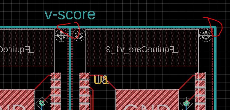
To re-size the V-Score lines,
you must select the line by selecting the tip of the line. Simply
clicking the line will not allow you to drag/resize the line in Eagle.
Selecting the tip by drawing a box around the tip as shown in the
following figure then resize it by clicking and holding one terminal of
the line.
The dimension line of each board in the panel should be deleted. Displaying the dimension as follows:
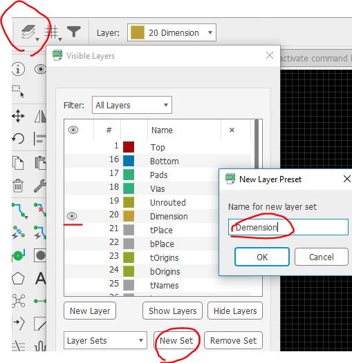
It shows the following view:
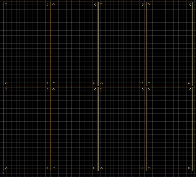
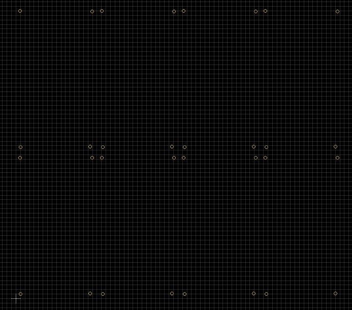
Delete the dimension lines of each board (don't delete the through holes in the corners).
Resize the V-SCORE lines:
Draw the dimension of the entire board:
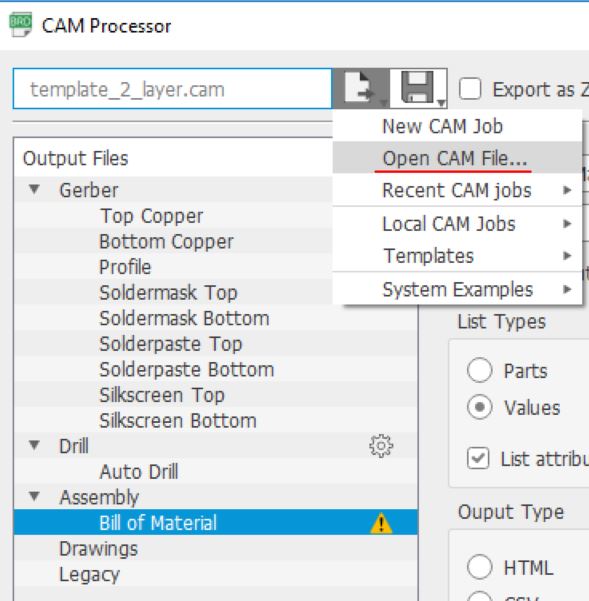
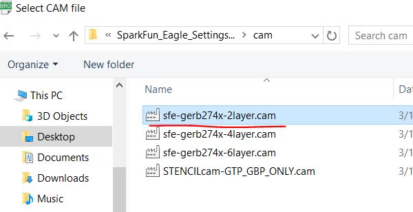
Export the gerber file using the following CAM proessor:
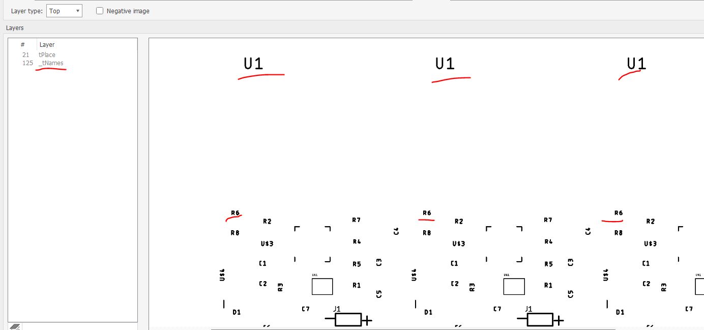
Make sure that the parts in
all boards have the same names. In the layers, delete the tName and
bName layers, add the _tName and _bName layers. The original tName and
bName layers keep the different names of the parts. However, the _tName
and _bName layers are the extracted names from panelization so they
show the same names.
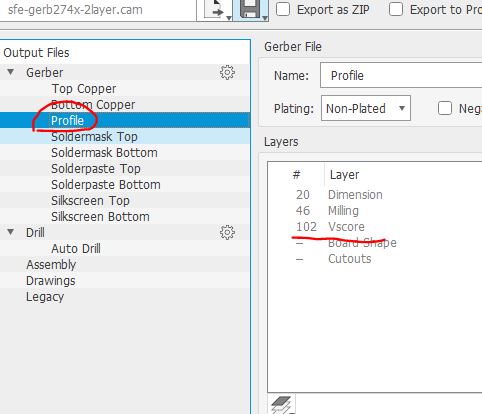
In the Profile layer (the cut layer), add Vscore and Milling in it.
Then export the Gerber files for fab.