ENGR337 Lab 2020 Spring
Lab 10 Complete Tutorial 5
James Ferguson
jwferguson@fortlewis.edu
Lab 9 Complete Tutorial 5
Introduction:
The
goal of this lab is to design an operational amplifier as well as gain
experience with the software ElectricVLSI. An operational amplifier
produces an output that is hundreds of times larger than the difference
between its two inputs. Using an operational amplifier along with
resistors and capacitors, electric signals can be filtered and
amplified. This op-amp will be placed inside a chip layout with electro
static discharge protection along with an inverter.
Methods:
ElectricVLSI was setup prior to starting following the same procedure as in Lab 6. This report follows instructions found in Tutorial 5: Complete the Op Amp IC on Dr. Li's website. The following figures show the schematic and layout of all the components used to in this chip layout.
Capacitor:
Bias:
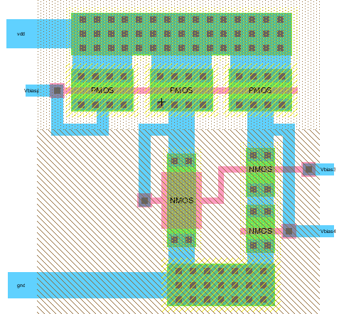
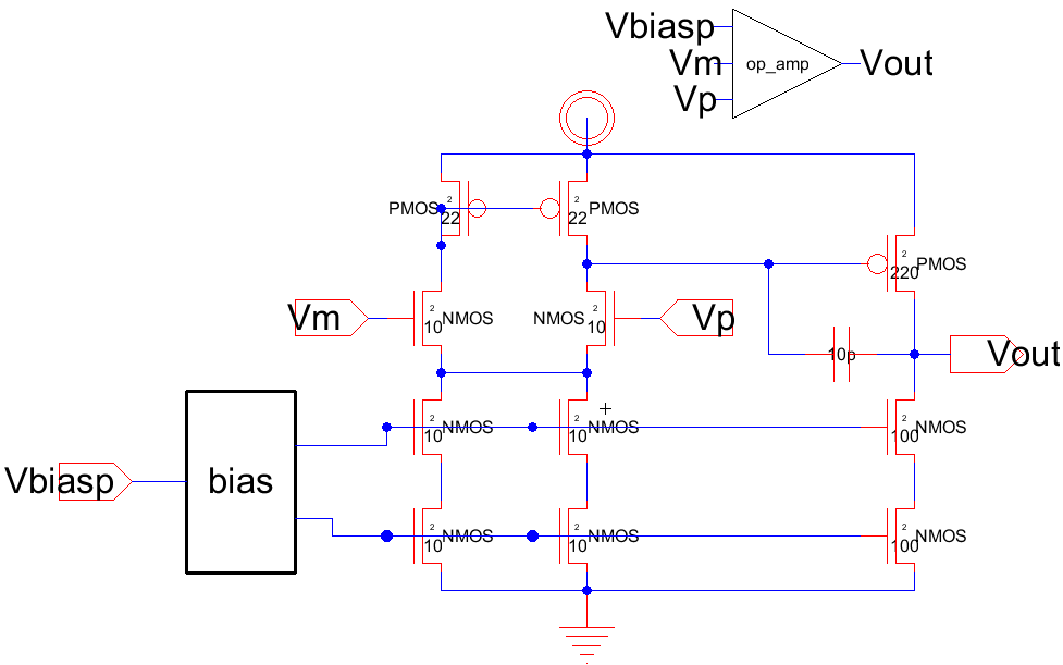
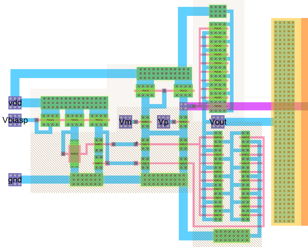
Op Amp:
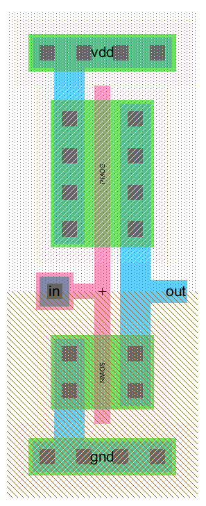
Inverter:
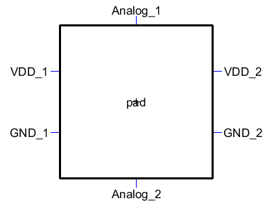
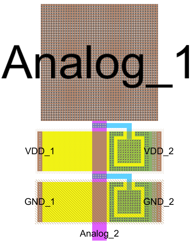
Pad:
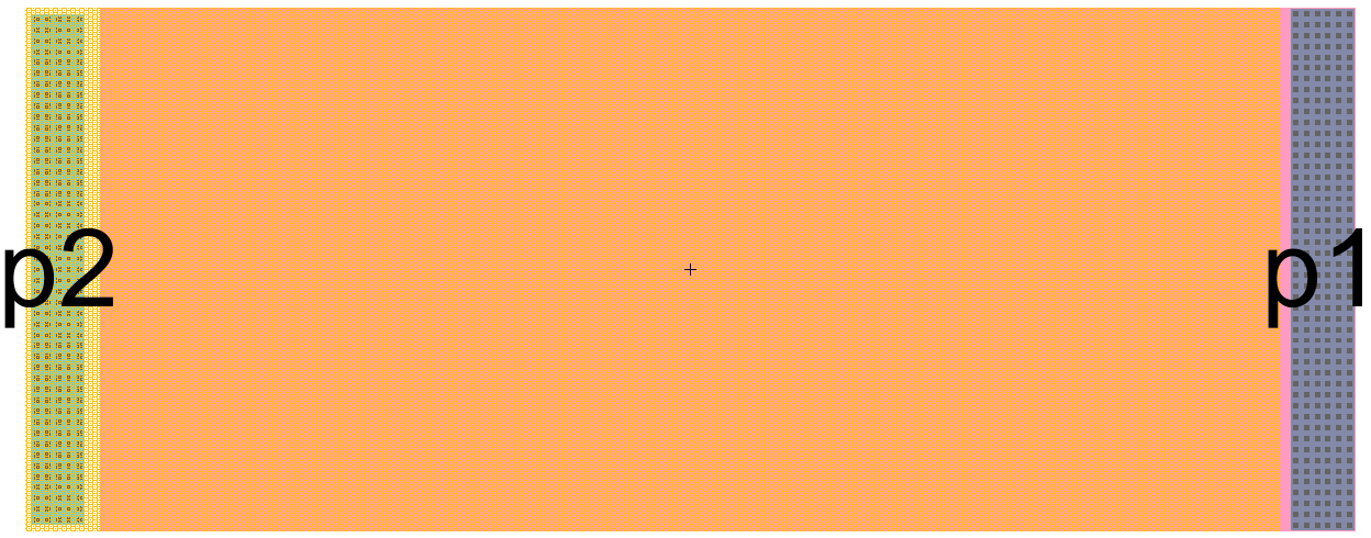
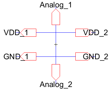
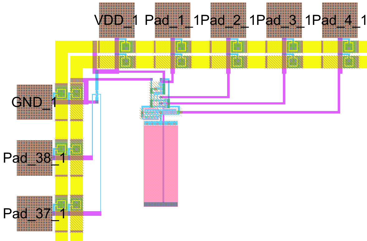
Pad Frame:
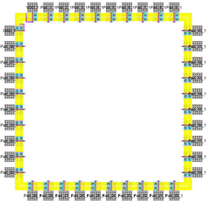
Op Amp Pad Frame:
Results:
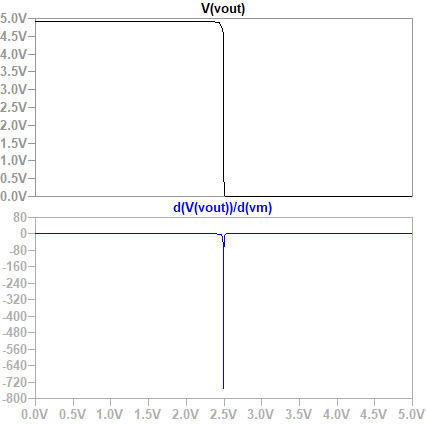
Through a LTspice simulation the open-loop gain of this op-amp was found to be around -720dB.

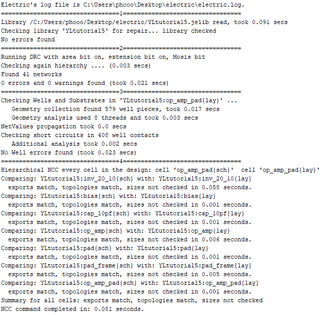
Schematic and layout passed DRC, ERC and NCC checks without any errors.
Conclusion:
All layout and
schematics passed DRC, ERC, and NCC tests without any errors and appear to
be usable. The open-loop of the designed circuit is several orders of magnitude
smaller compared to popular commercially available op-amps. This means that
this design could be significantly improved upon in further studies.