In this
Tutorial, we will put 3 Op Amps and 3 inverters into your padframe.
Let's finalize
the Op Amp design first.
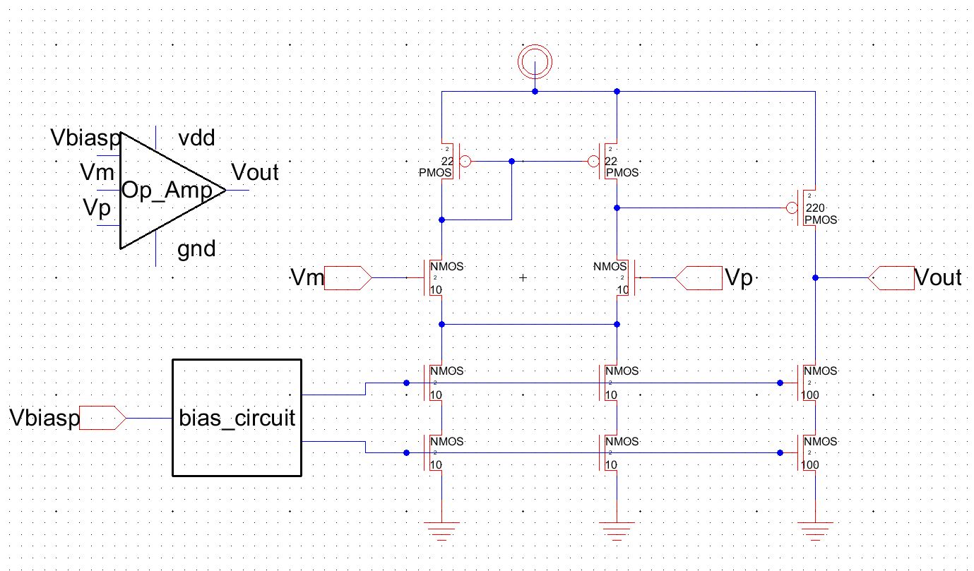
5.1 Understand the Op Amp Circuit.
Video 1: Watch the following video to understand the operation of the Op Amp. (PDF notes)
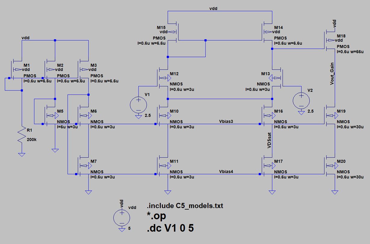
All
the DC operating points are set up when the off-chip resistor is around
200k. The open loop gain can be simulated use the following circuit and
Spice code:
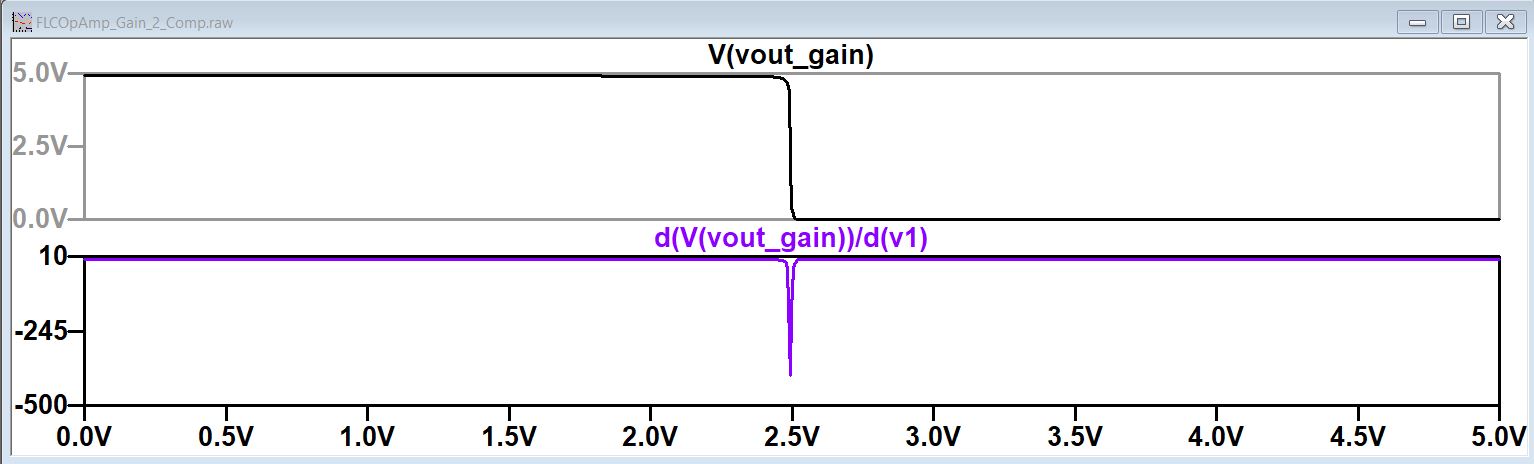
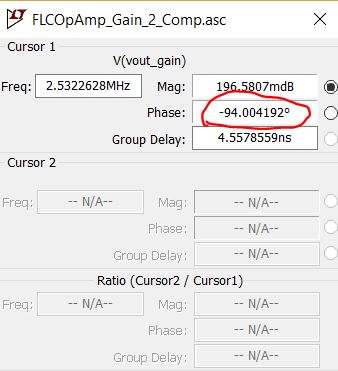
The results can
be presented like the following:
The second
diagraph shows the open loop gain is around -400.
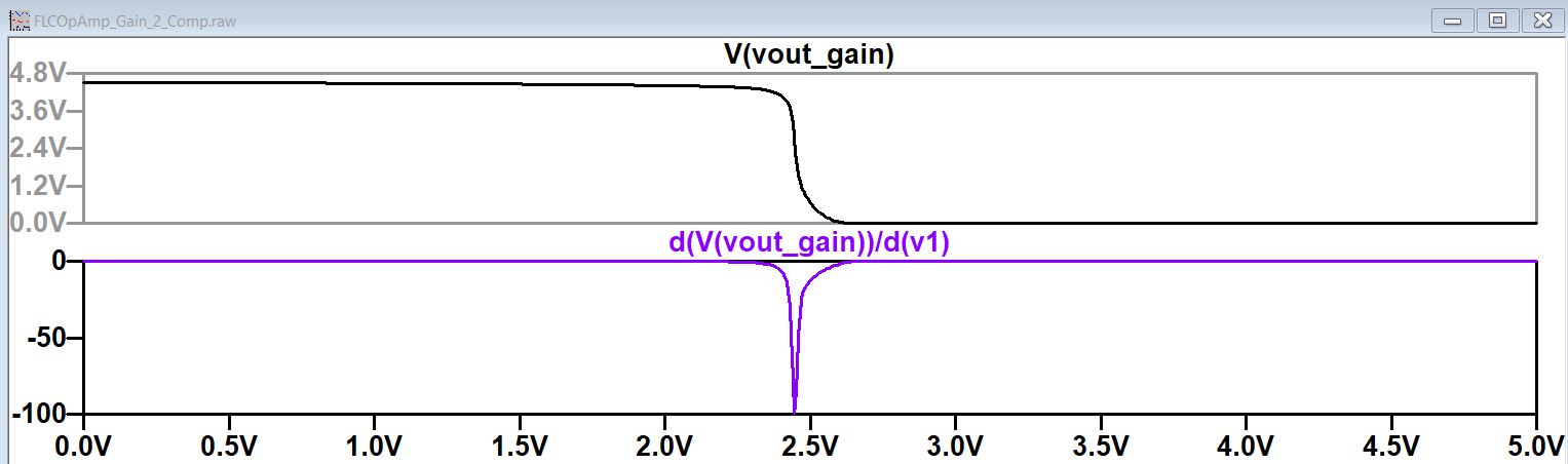
However,
if the CMOS transistors are not biased in the saturation region, the
gain will decrease and the Op Amp cannot work correctly. I changed the
resistor to 10k, you will see the drop of the grain:
(This part is not required for ENGR 337 students)----->>
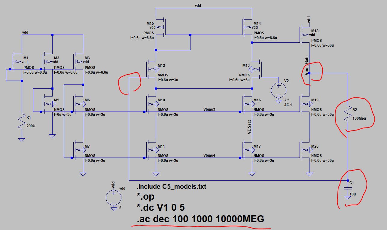
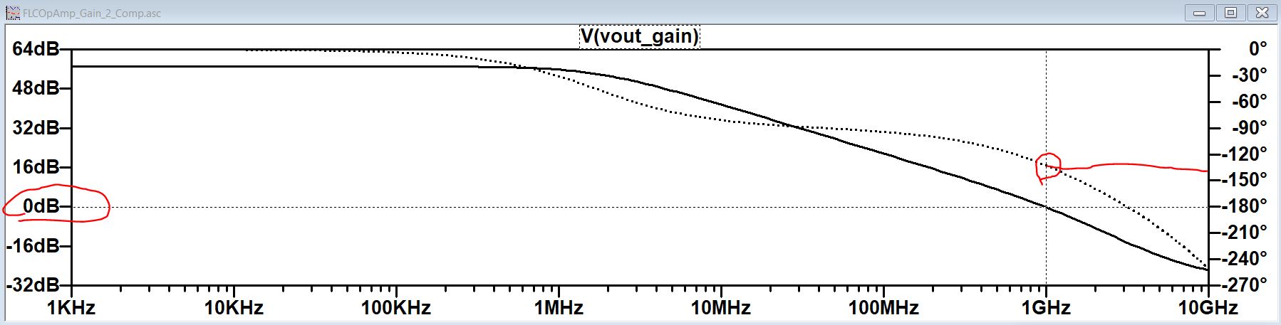
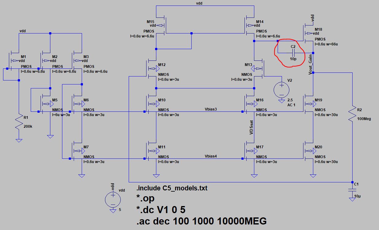
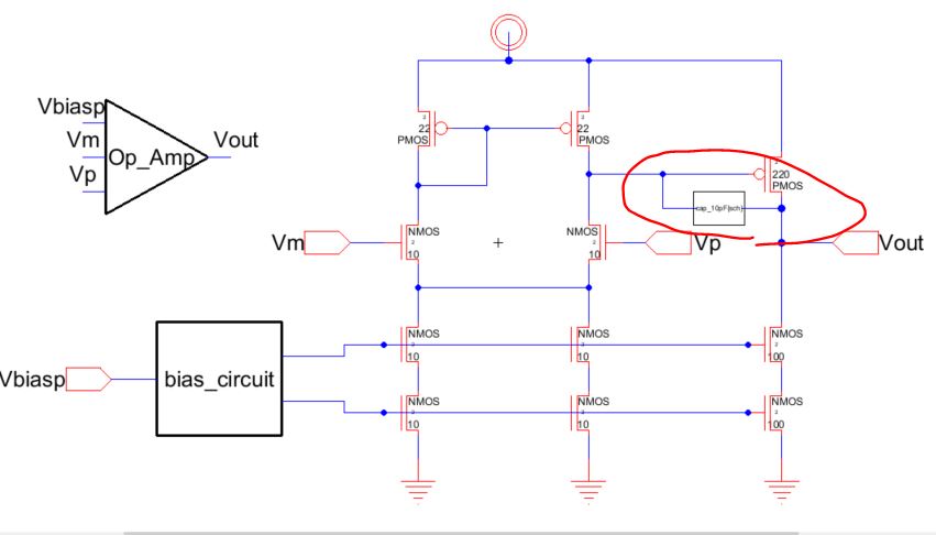
Now
let's add a capacitor from the output of the second stage to the output
of the differential pair to improve the stability of the Op Amp. Here
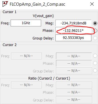
is a new concept - Phase Margin. In frequency response of the Op Amp,
when the gain of the Op Amp is 0 dB, the phase difference from this
point to -180 degree is the Phase margin. 90 degree of phase margin is
usually ideal (CMOS Book Chapter 24). However, if we don't add the 10
pF capacitor, the phase margin is around 40 degree (not that stable):
(note that the 100 MEG resistor is used to conduct the DC bias but
blcok any AC component and the 10 uF capacitor is used to remove any AC
noise).
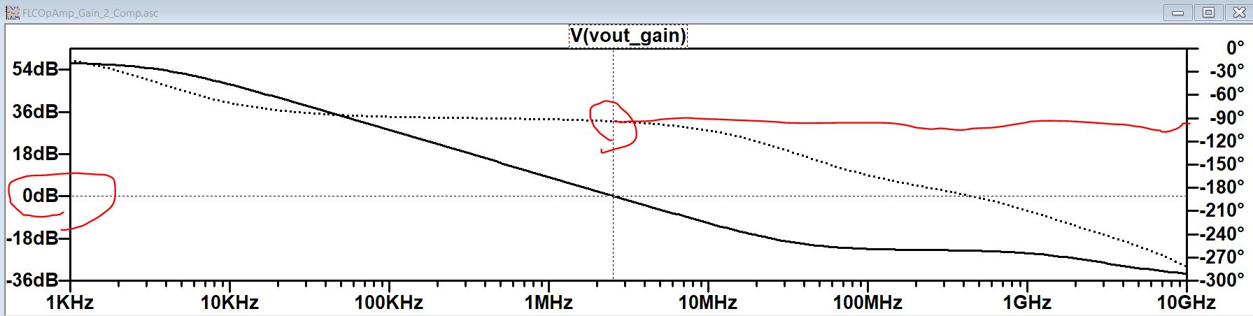
When we have the
10 pF 'compensating capacitor' added, the phase margin is pretty close
to 90 degree!
<<------- (This part is not required for ENGR 337 students)
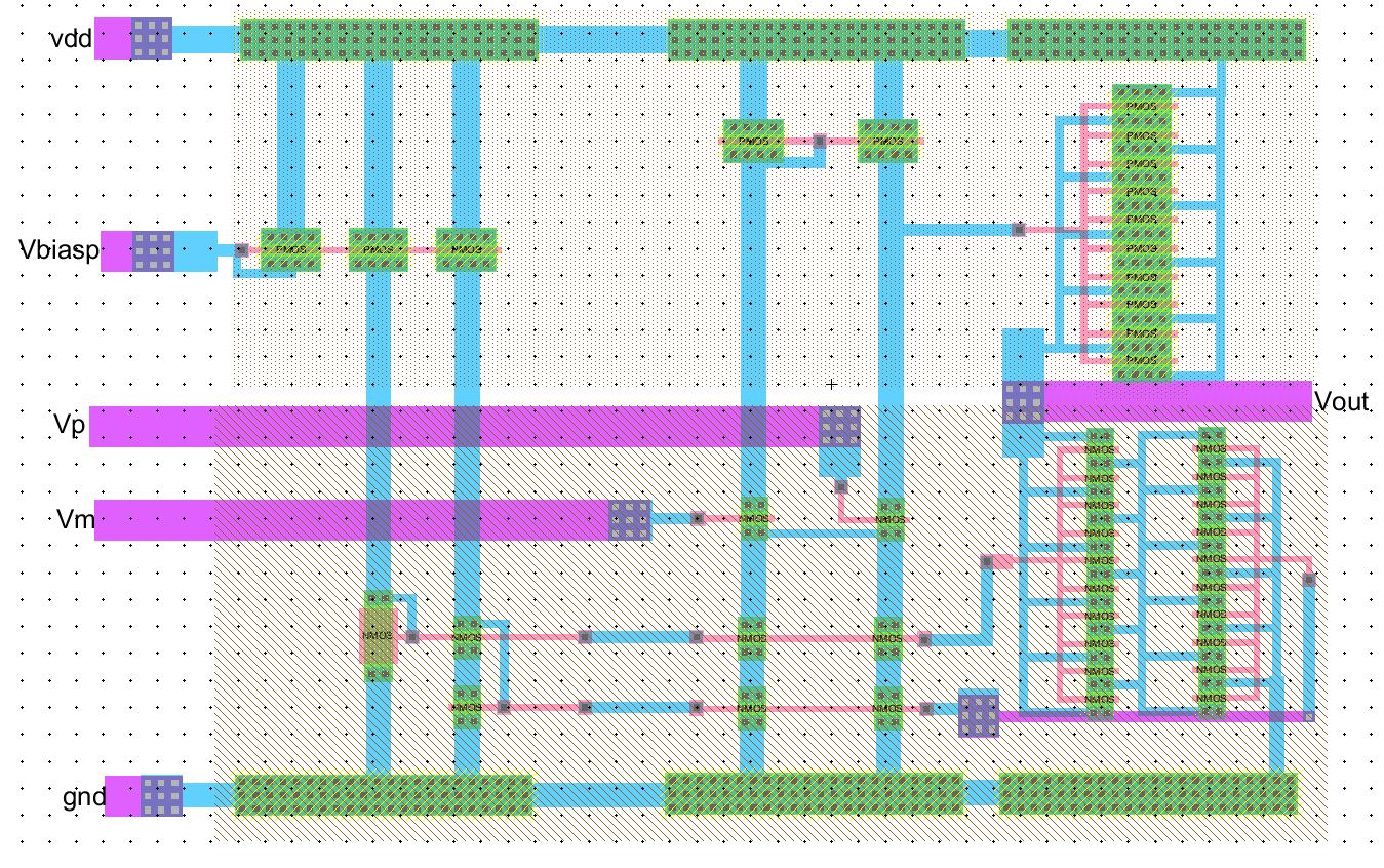
5.2 Layout the Biasing Circuit and the Op Amp Video 2: Layout the Biasing Circuit:
Video 3: Layout an Op Amp:
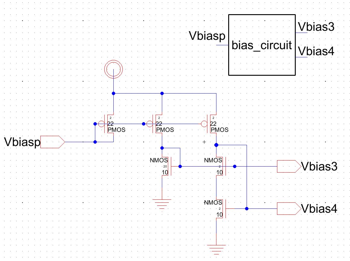
Make the
schematic and icon view for the bias_circuit:
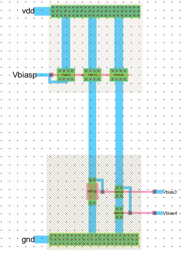
Make the layout view of the bias_circuit. Note that the PMOS and nWell
should be covered in the region of a Pure N-Well-Node (Components -
Pure - N-Well-Node).
The size of
N-Well-Node can be re-sized using the 'special click' and click 'y'.
The same concept
applied to the NMOS, the PWell and the P-Well-Node.
In the Op_Amp
library, draw the schematic and icon: (Use the bias_circuit icon in
your Op Amp circuit).
Create the layout of the Op Amp (drag the bias_circuit layout into your
Op Amp layout). Make sure you have ZERO DRC/NCC/ERC errors. Copy
the screenshot of the message window which has the DRC and LVS
clean messages for credit.
Video 4: Wrap Up the Chip Layout:
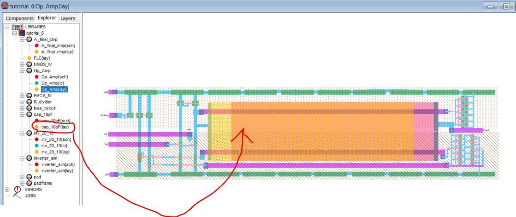
Now let's add
the 10 pF capacitor to your layout:
Create
a layout view of the capacitor. The total area of the capacitor should
be 130,000 by scale. So measure the distance between the vdd rail and
the gnd rail before you the length of the material is determined.
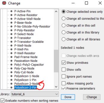
Start
with P2 material. Grab a poly-2 pin and change the dimenion to your
desired dimension but a little bit longer (to fit the metal 1 - poly 2
contact to it). Then select the pin and press 'c' to change it into a
poly-2 node:
Don't
forget to add the poly - metal 1 contacts to the poly layers. Use the
ruler to double check if the dimension of the overlapped area is the
one you expected.
DRC and LVS the
schematic and the layout, make sure they match.
Go to your Op
Amp layout view, move the last stage to the right to fit the capacitor
in between. Connect all the circuits. (In the video, I added the capacitor the end of the Op Amp. Either way works).
Drag the
schematic of the capacitor into the schematic of your Op Amp:
!!!
Make sure you DRC and LVS your circuits after every step before
you move on, otherwise, you will find hundreds of errors in your final
circuit.
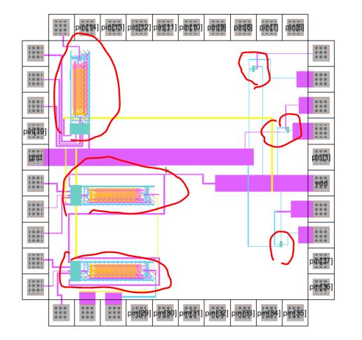
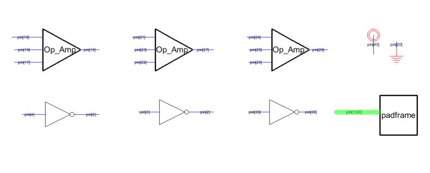
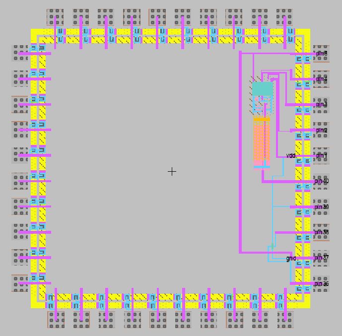
Now, put three
copies of the Op Amp and three copies of the inverters into your pad
frame: (This is the old padframe which does not have ESD protections).
Complete the
schematic of the chip:
(This is also for the old design. The new one is demonstrated in the
video. You can do either one for your project but the new one is
recommended).
Again,
DRC/LVS your final design for credit.
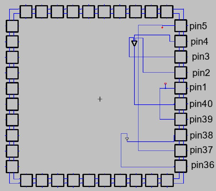
If you followed the tutorial in the video, your final chip layout looks like this:
Your schematic looks like this:
Requirements
for the final report: 1.
Have the DC operating point simulation data organized in a table. Show
the correct resistor value that can make all the transistors in
saturation region. 2. Show the
open-loop gain of the Op Amp. 3. Show the
schematic and layout view of every component and the final chip view. 4. Show the DRC and LVS clean (screen shot for the final chip.