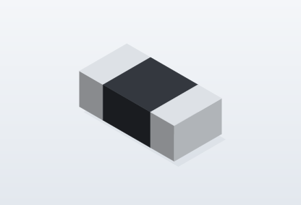
01005Metric 0402
- Size
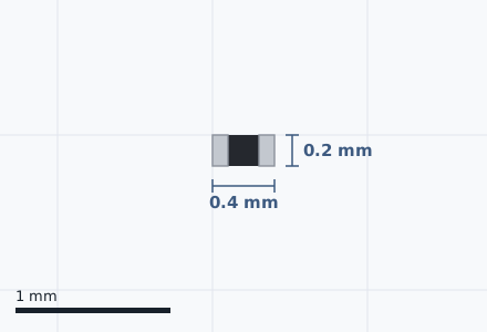
- 0.4 × 0.2 mm
- Leads
- 2 terminals
- Power
- 1/32 W
- Hand soldering
- Reflow only
- Typical use
- Phones, wearables
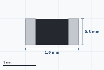
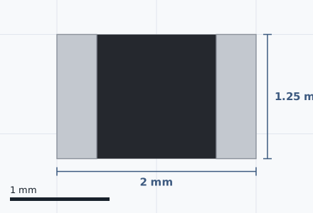
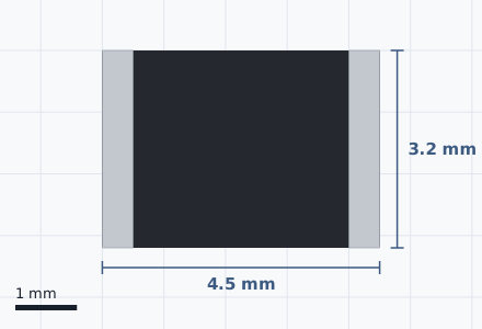
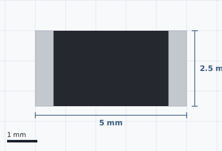
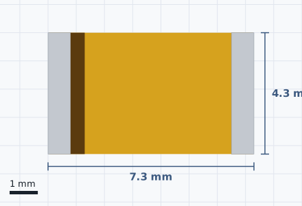
Dimensioned top view, to scale
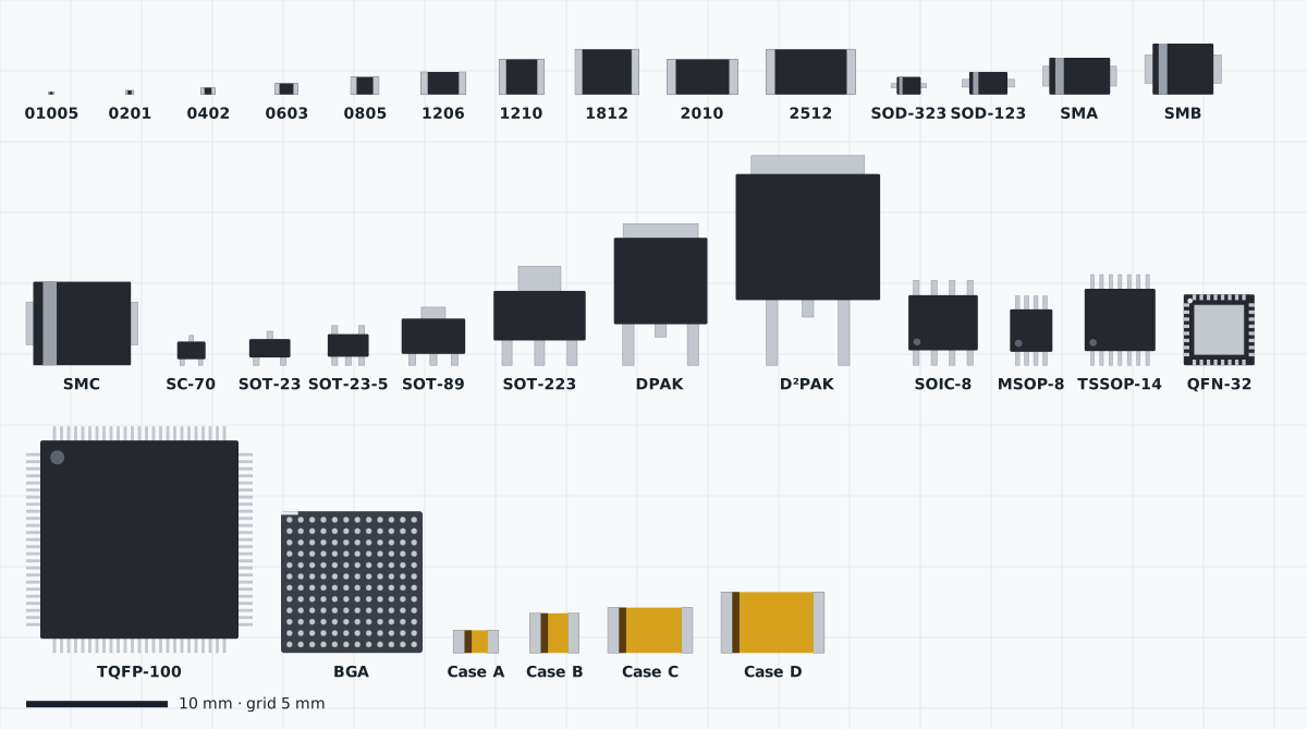
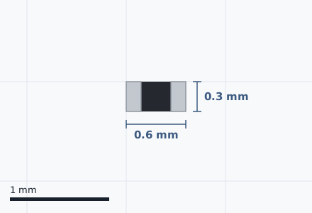
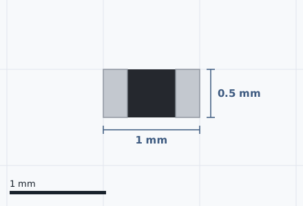
Thirty-two common surface-mount packages: what each looks like, how big it really is and how much power it can handle, plus polarity marks, part codes and the rules of thumb every board designer needs. Written for CE351 alongside the Skyboard lectures. Each card’s picture is enlarged to fill the card; the lineup below and the dimensioned drawings show true size.
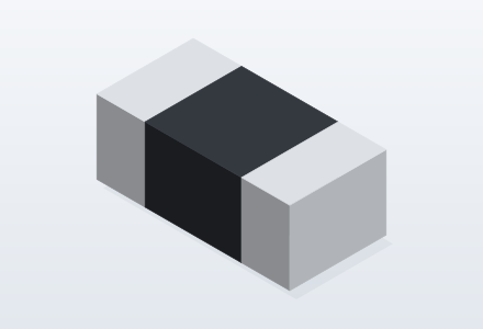
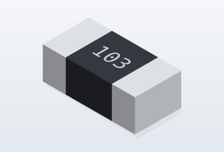
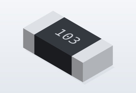
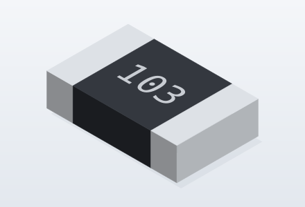
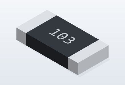
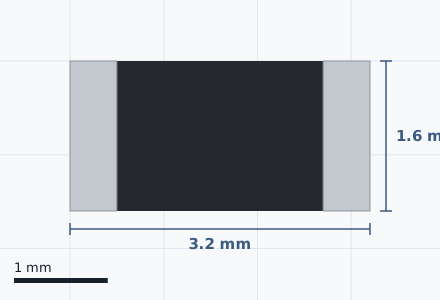
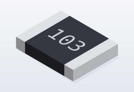
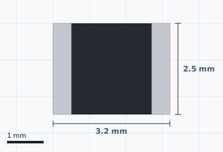
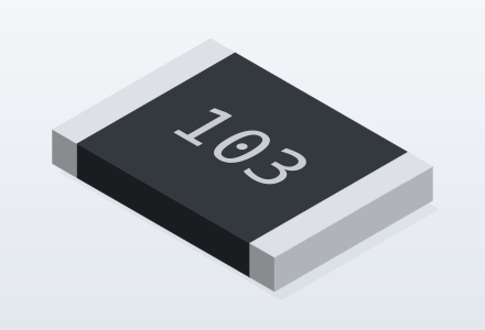
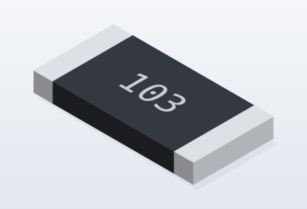
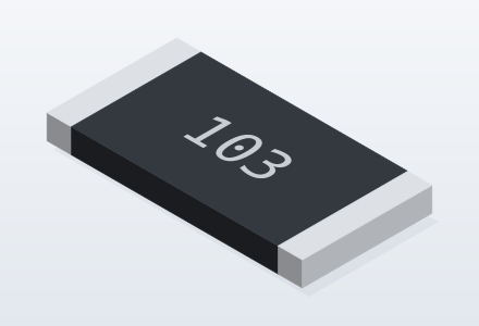
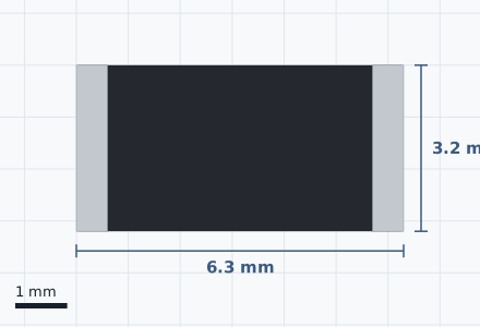
Two metal end caps on a ceramic body. The name is the size code: imperial 0805 means 0.08 × 0.05 inch. Capacitors use the same sizes with a tan or grey body. Power ratings are standard thick-film resistor values at 70 °C ambient.
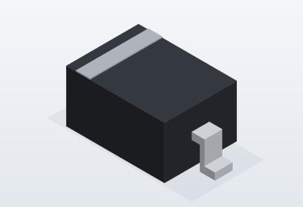
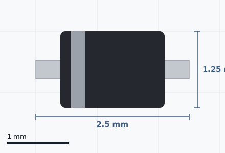
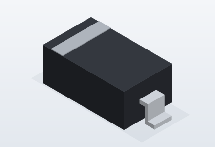
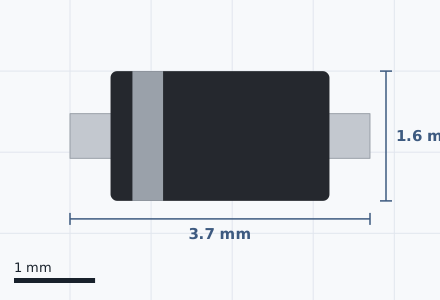
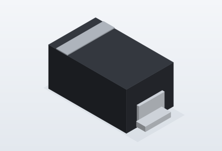
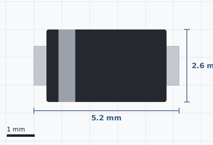
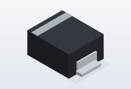
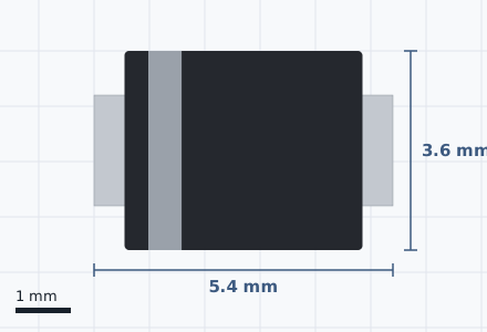
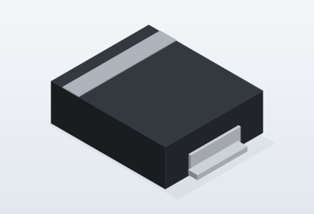
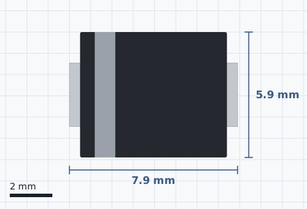
Two-terminal packages with a band marking the cathode. SOD parts have small gull-wing leads; SMA, SMB and SMC have J-leads folded under the body and are rated by current and surge power.
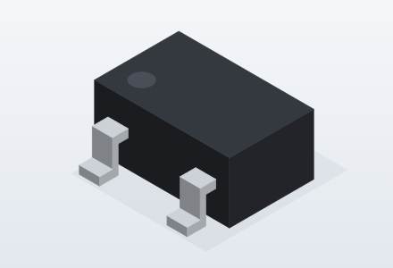
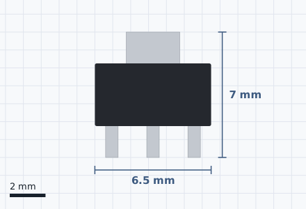
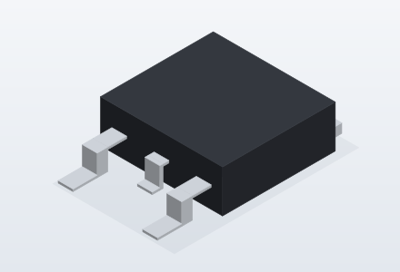
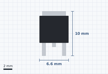
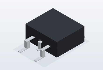
Three to six leads, with a metal tab on the larger packages. The tab is soldered to a copper area that spreads the heat, so the power figure depends on how much copper you give it.
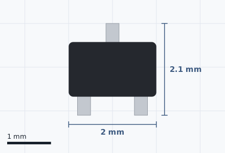
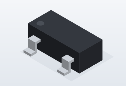
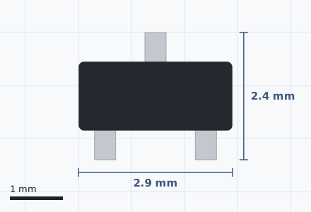
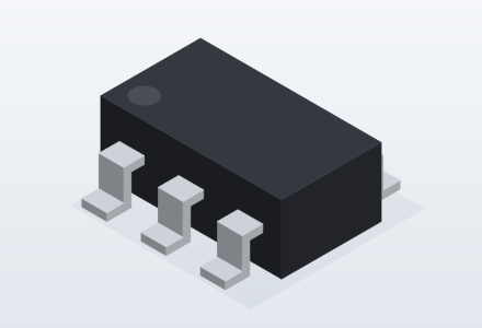
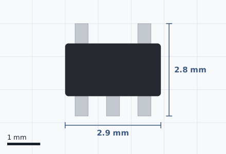
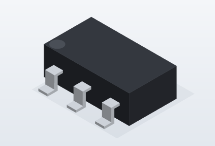
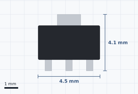
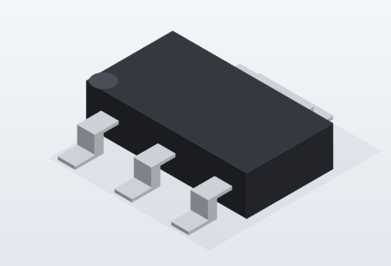
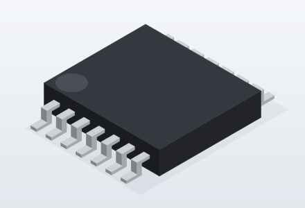
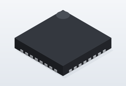
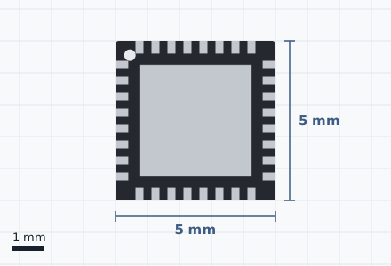
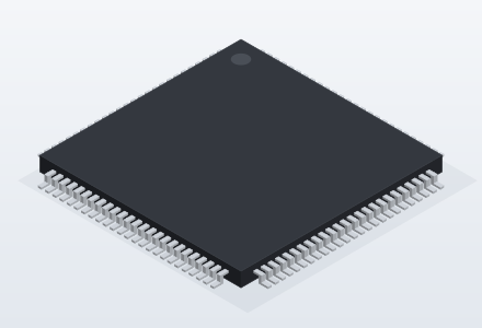
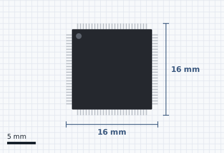
Leaded packages (SOIC, MSOP, TSSOP, QFP) can be inspected and reworked with an iron. Leadless QFN and BGA packages are smaller and run cooler, but need a stencil and reflow or hot air.
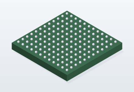
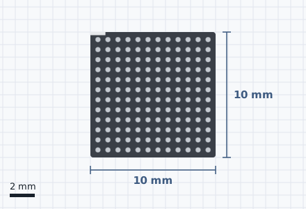
Shown upside down so the solder balls are visible.
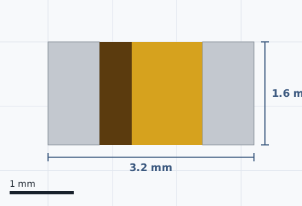
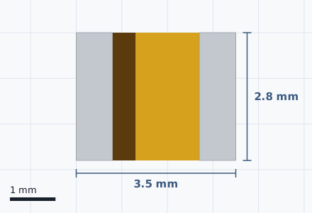
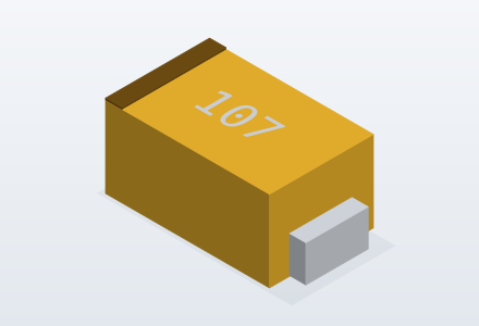
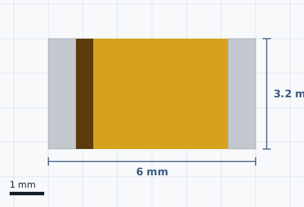
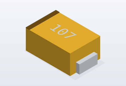
Polarised capacitors in letter-coded cases. The band marks the positive (anode) end, the opposite of a diode band. They are limited by voltage and ripple current rather than a power rating.
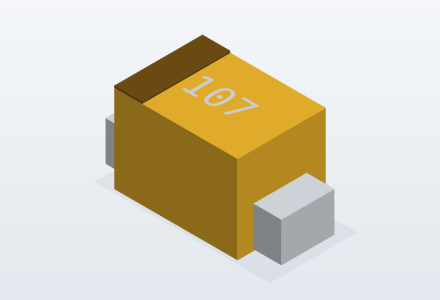
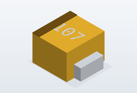
Most first-board failures are a part soldered the wrong way round. Learn these marks, put matching marks in your silkscreen, and check them against the datasheet before ordering.
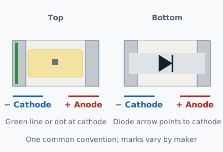
Look for a green line, dot or notch on the top, or a diode arrow on the bottom; the arrow points to the cathode. Conventions differ between makers, so confirm with the datasheet or a multimeter’s diode mode: the LED glows faintly when the red probe is on the anode.
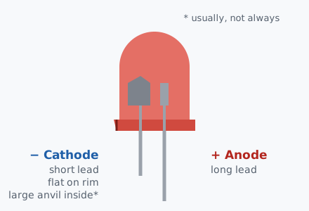
The anode has the longer lead. The cathode side has a flat on the rim and usually the larger anvil inside. Once the leads are trimmed, the flat is the mark that remains.
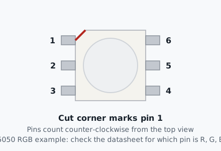
A cut corner, dot or triangle marks pin 1. Common-anode and common-cathode versions look identical, and colour-to-pin order varies, so read the pinout table every time.
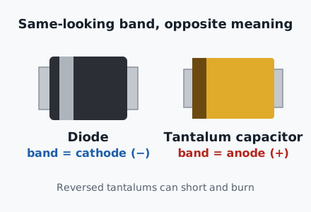
The classic trap: a diode band marks the cathode (−), but a tantalum capacitor band marks the anode (+). A reversed tantalum can fail short and catch fire.
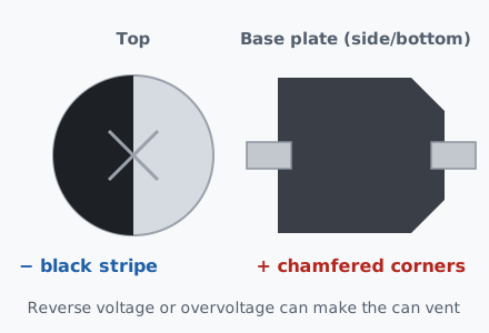
The black stripe on top marks negative. On the plastic base, the chamfered corners are on the positive side. Footprints usually copy that outline in silkscreen.
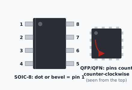
Pin 1 is next to the dot, dimple or bevelled edge. Pins then count counter-clockwise viewed from the top. Large dots can be mould marks: if there are two, the smaller one is usually pin 1.
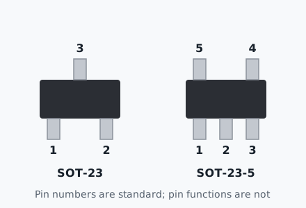
Pin numbering is fixed, but the function is not: one SOT-23 transistor may be B-E-C and another G-S-D in a different order. Never assume a pinout from the package.
Small parts carry codes instead of values. Many ceramic capacitors carry no marking at all, so keep them in labelled tape or bags.
| Marking | Part | How to read it | Value |
|---|---|---|---|
| 103 | Resistor, 3-digit | 10 × 10³ | 10 kΩ (5%) |
| 472 | Resistor, 3-digit | 47 × 10² | 4.7 kΩ |
| 4R7 · R47 | Resistor | R is the decimal point | 4.7 Ω · 0.47 Ω |
| 1002 | Resistor, 4-digit | 100 × 10² | 10.0 kΩ (1%) |
| 01C | Resistor, EIA-96 | Code 01 = 100, letter C = × 100 | 10.0 kΩ (1%) |
| 0 or 000 | Zero-ohm link | A jumper in resistor form | ≈ 0 Ω |
| 107 · 6V | Tantalum capacitor | 10 × 10⁷ pF, then rated voltage | 100 µF, 6.3 V |
| 47 · 25V | Electrolytic can | Value printed directly | 47 µF, 25 V |
| 100 · 4R7 | Inductor | Code in µH | 10 µH · 4.7 µH |
| Ceramic dielectric | Temperature range | Change over temperature | Use it for |
|---|---|---|---|
| C0G / NP0 | −55 to +125 °C | ±30 ppm/°C, no voltage loss | Crystal load caps, filters, timing (pF to ~nF) |
| X7R | −55 to +125 °C | ±15% | General decoupling |
| X5R | −55 to +85 °C | ±15% | High-value decoupling in small cases |
| Y5V / Z5U | −30 to +85 °C | +22 / −82% | Avoid in new designs |
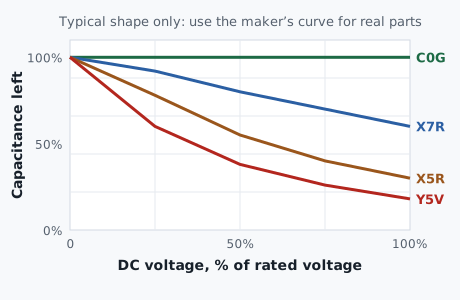
Class 2 ceramics (X7R, X5R, Y5V) lose capacitance as DC voltage is applied. A 10 µF, 6.3 V, 0603 X5R part on a 5 V rail may deliver only a third of its label value.
Use a higher voltage rating or a larger case to keep more of it, and check the manufacturer’s DC-bias curve for the exact part. C0G parts do not have this effect, which is why they are used for crystals and filters.
R = (Vsupply − Vf) / If
Red from 5 V at 10 mA: (5 − 2.0) / 0.01 = 300 Ω, so use 330 Ω. Give each LED its own resistor rather than sharing one across parallel LEDs.
| Colour | Typical Vf |
|---|---|
| Infrared | 1.2–1.5 V |
| Red | 1.8–2.2 V |
| Yellow / orange | 2.0–2.2 V |
| Green (InGaN), blue, white | 2.8–3.4 V |
Tantalum (MnO₂): use a part rated about twice the working voltage, e.g. 10 V on a 5 V rail, and limit inrush. Polymer: about 20% margin. Electrolytic: life roughly halves for every 10 °C hotter, so keep them away from regulators and power resistors.
C1 = C2 ≈ 2 × (CL − Cstray)
CL is on the crystal datasheet; stray capacitance is typically 2–5 pF. A 15 pF crystal with 4 pF stray needs ≈ 22 pF, the value on the Skyboard 16U2 crystal. Use C0G parts.
MOSFETs, CMOS ICs and LEDs can be damaged by a discharge you cannot feel. Use a wrist strap and mat, keep parts in their antistatic bags until placement, and touch ground before handling a board.
Plastic packages absorb moisture. Check the MSL rating on the reel bag: if a level 3 part has been out longer than its floor life (168 hours), bake it before reflow, or it can crack inside (“popcorning”).
Small passives can stand on one end during reflow when one pad heats faster. Keep both pads the same size, connect them with equal trace widths, and use thermal relief on pour connections.
A PTC’s hold current is what it carries forever; trip current is usually about double, and tripping takes time. Hold current falls as the board heats up. Skyboard’s F1 holds 500 mA at room temperature.
Print the layout 1:1 and lay real parts on it. Check pin 1 and polarity marks against the datasheet, view the 3D model, and make sure the silkscreen marks stay visible after the part is placed.
P = (TJ,max − TA) / θJA
Transistor and IC packages do not have a fixed power rating. The chip can run up to its maximum junction temperature, usually 125–150 °C, and θJA (°C per watt, from the datasheet) says how fast heat escapes to the air.
Example: a SOT-23 at about 350 °C/W on minimum pads, 150 °C junction, 25 °C room: (150 − 25) / 350 ≈ 0.36 W.
Copper is the heatsink
Packages with a tab or exposed pad (SOT-223, DPAK, QFN) move most of their heat into the board. A larger copper pour and thermal vias to the other layer can lower θJA by half or more, which is how a DPAK reaches several watts.
Chip resistors are rated at 70 °C ambient and derate linearly to zero at about 155 °C. Keep at least a 2× margin in practice.
| Package | Also called | Size | Leads / pitch | Typical power | Hand soldering |
|---|---|---|---|---|---|
| 01005 | Metric 0402 | 0.4 × 0.2 mm | 2 terminals | 1/32 W | Reflow only |
| 0201 | Metric 0603 | 0.6 × 0.3 mm | 2 terminals | 1/20 W | Reflow only |
| 0402 | Metric 1005 | 1.0 × 0.5 mm | 2 terminals | 1/16 W | Hard |
| 0603 | Metric 1608 | 1.6 × 0.8 mm | 2 terminals | 1/10 W | Moderate |
| 0805 | Metric 2012 | 2.0 × 1.25 mm | 2 terminals | 1/8 W | Easy |
| 1206 | Metric 3216 | 3.2 × 1.6 mm | 2 terminals | 1/4 W | Easy |
| 1210 | Metric 3225 | 3.2 × 2.5 mm | 2 terminals | 1/3–1/2 W | Easy |
| 1812 | Metric 4532 | 4.5 × 3.2 mm | 2 terminals | 1/2–3/4 W | Easy |
| 2010 | Metric 5025 | 5.0 × 2.5 mm | 2 terminals | 3/4 W | Easy |
| 2512 | Metric 6332 | 6.3 × 3.2 mm | 2 terminals | 1 W (2–3 W special series) | Easy |
| SOD-323 | SC-76 | 1.7 × 1.25 mm body | 2 leads | 0.2–0.3 W | Moderate |
| SOD-123 | 2.7 × 1.6 mm body | 2 leads | 0.4–0.5 W | Easy | |
| SMA | DO-214AC | 4.3 × 2.6 mm body | 2 J-leads | ≈1 A diode; 400 W TVS pulse | Easy |
| SMB | DO-214AA | 4.3 × 3.6 mm body | 2 J-leads | 2–3 A; 600 W TVS pulse | Easy |
| SMC | DO-214AB | 6.9 × 5.9 mm body | 2 J-leads | 3–5 A; 1500 W TVS pulse | Easy |
| SC-70 | SOT-323 | 2.0 × 1.25 mm body | 3–6 leads, 0.65 mm | 0.15–0.2 W | Hard |
| SOT-23 | TO-236 | 2.9 × 1.3 mm body | 3 leads, 0.95 mm | 0.2–0.35 W | Moderate |
| SOT-23-5 | SC-74A | 2.9 × 1.6 mm body | 5 leads, 0.95 mm | 0.2–0.4 W | Moderate |
| SOT-89 | 4.5 × 2.5 mm body | 3 leads, 1.5 mm | 0.5–1 W | Easy | |
| SOT-223 | TO-261 | 6.5 × 3.5 mm body | 3 leads + tab, 2.3 mm | 1–2 W | Easy |
| DPAK | TO-252 | 6.6 × 6.1 mm body | 2 leads + tab, 4.57 mm | 2–3 W on a copper pad | Easy |
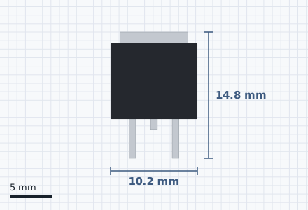
| D²PAK | TO-263 | 10.2 × 8.9 mm body | 2–3 leads + tab, 5.08 mm | 3–5 W on a copper pad | Easy (large iron) |
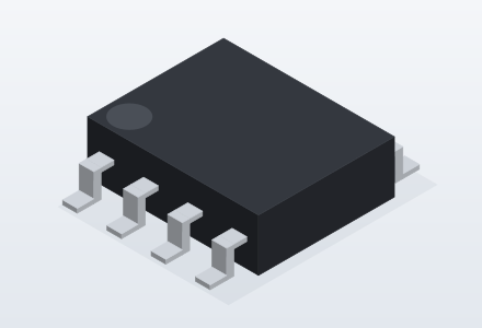
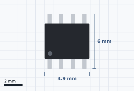
| SOIC-8 | SO-8 | 4.9 × 3.9 mm body, 6.0 mm with leads | 8 leads, 1.27 mm | 0.5–1 W | Easy |
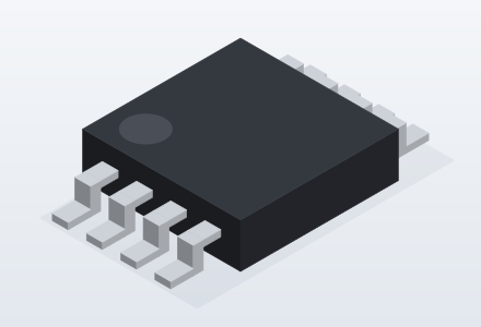
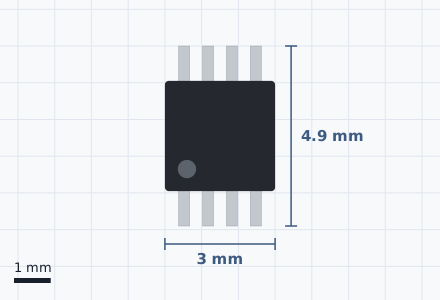
| MSOP-8 | VSSOP-8 | 3.0 × 3.0 mm body | 8 leads, 0.65 mm | 0.4–0.6 W | Moderate |
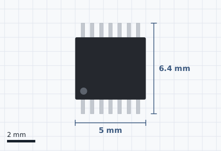
| TSSOP-14 | 5.0 × 4.4 mm body | 14 leads, 0.65 mm | 0.5–1 W | Moderate | |
| QFN-32 | 5 × 5 mm | 5.0 × 5.0 mm | 32 pads, 0.5 mm, exposed pad | 1–3 W with thermal vias | Hard (hot air) |
| TQFP-100 | 14 × 14 mm | 14 × 14 mm body, 16 mm with leads | 100 leads, 0.5 mm | 0.7–1.5 W | Moderate (drag solder) |
| BGA (example) | 10 × 10 mm, 0.8 mm pitch | 10 × 10 mm (sizes vary widely) | 144 balls, 0.8 mm | 1 W to tens of W with heatsink | Reflow only |
| Case A | EIA 3216 | 3.2 × 1.6 mm | 2 terminals, polarised | Rated by voltage and ripple current | Easy |
| Case B | EIA 3528 | 3.5 × 2.8 mm | 2 terminals, polarised | Rated by voltage and ripple current | Easy |
| Case C | EIA 6032 | 6.0 × 3.2 mm | 2 terminals, polarised | Rated by voltage and ripple current | Easy |
| Case D | EIA 7343 | 7.3 × 4.3 mm | 2 terminals, polarised | Rated by voltage and ripple current | Easy |