Tutorial
5: Ring Oscillator
Copy the library,
Tutorial_4, into a new library called Tutorial_5.
Ensure that when you copy that
“update instances” is selected so that the new library doesn’t
reference cells in the other libraries.
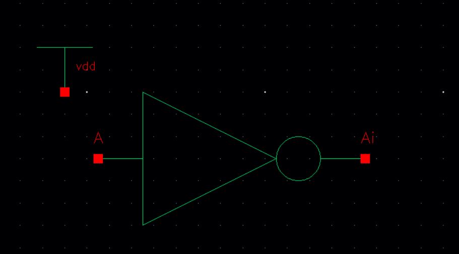
In Tutorial_4 create a
new schematic cell view called ring_osc. In this view place the
inverter symbol. And place a vdd.
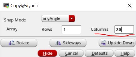
Next, select the
inverter and press "c". Before placing the inverter change the
columns to 30. We do this because a ring oscillator needs 31
inverters.
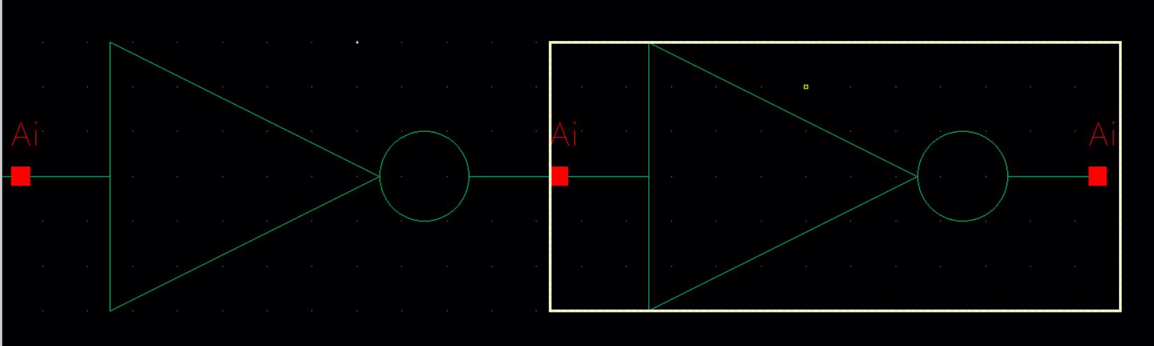
Place the inverters so the input of one is the output of the other.

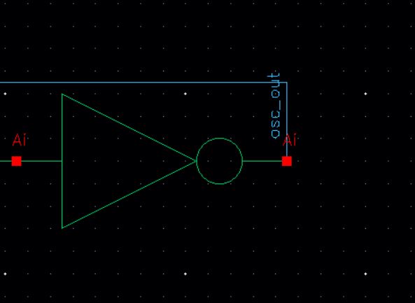
Add a wire connecting the output of the last inverter to the input of
the first inverter. Label the wire "osc_out". Then check and
save.

Now we will simulate the schematic, open ADE L and set up the
simulation. Add the nmos and the pmos models(aka MOSFET
models). And set the global stimuli to 5V. The output to
plot is wire osc_out. Set the analysis to transient and a length
of 200ns.
Please review tutorials 3 and 4 if you need assistance.
Save the state as a cellview then run the simulation.
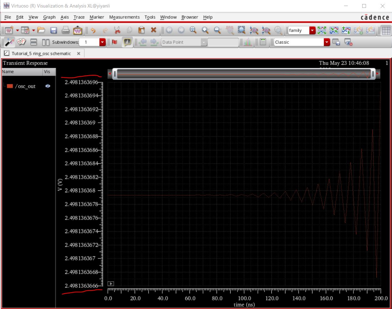
As we can see there is some oscillation, however when we look at the y
axis we can see that the scale of the oscillations is incredibly
small. If we did not have 8 decimals of accuracy then we would be
unable to see this oscillation. If we round to 3 sigfigs we see that
the output is really is 2.5V.
In real life the noise would kick-start the oscillations.
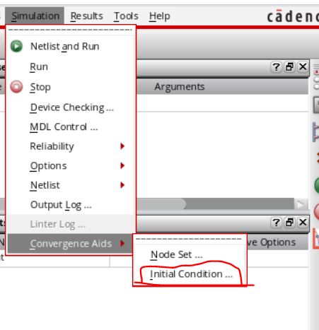
Lets do this by adding an initial condition. Mouse over to
"Simulation" then to "Convergence Aids" and click on "Initial
Condition".
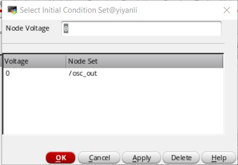
Have the node voltage set to 0 then select the output wire by clicking it in the schematic. Save
the state.
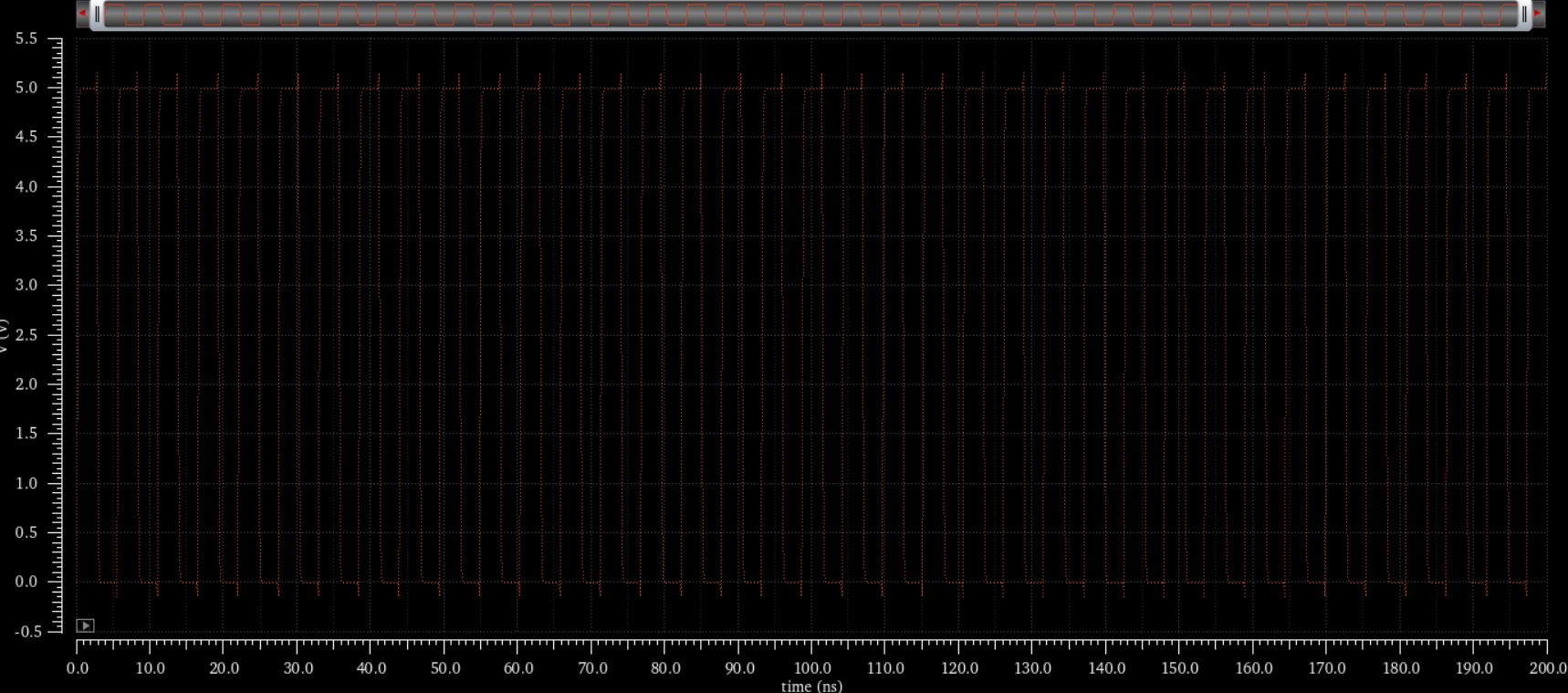
Running the simulation this time we get:
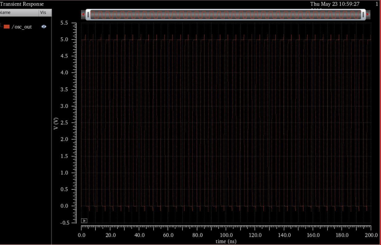
This is what a ring oscillator is supposed to do.
Save the state and close ADE.
It is very messy the way we have the 31 inverters in the schematic
right now. We are now going to clean it up and make it look much
more concise.
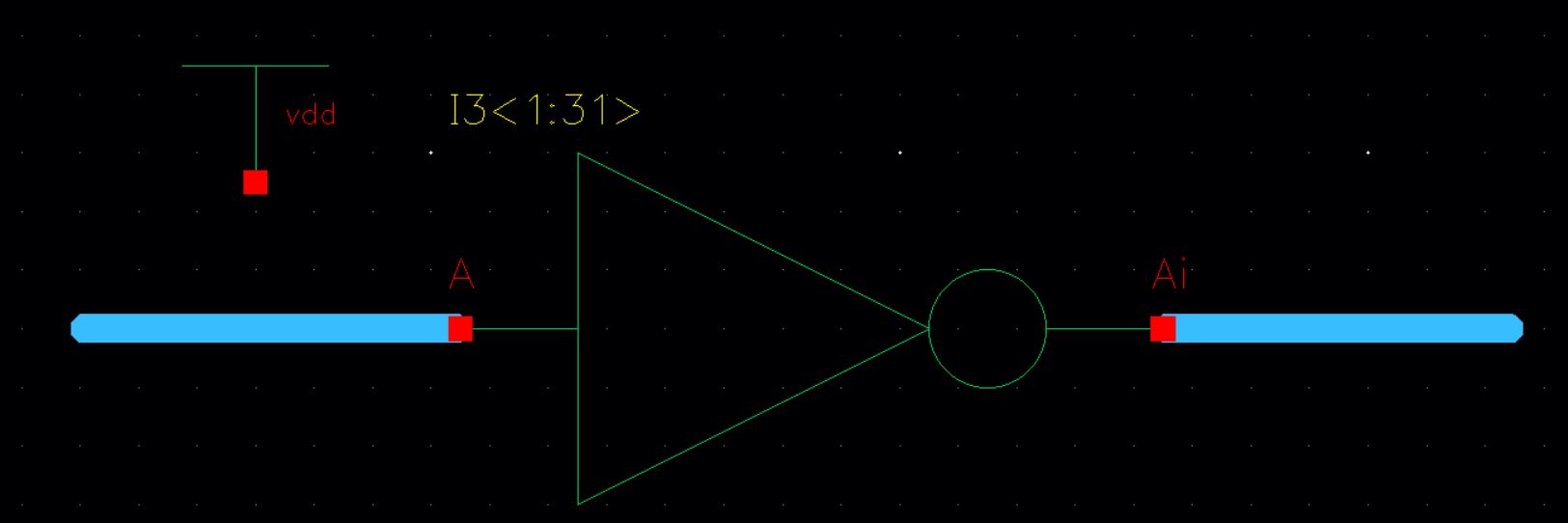
First, delete all but one of the inverts. Also delete all of the wires.
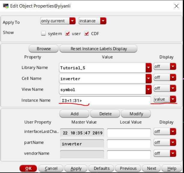
Next, change the name of the inverter to ( in my case)
I3<1:31>.
<1:31> means an array of 31 inverters. Then change the
Display to value.
To wire everything together type "W" or click on  .
This is a wide wire.
.
This is a wide wire.
Name the wires as seen below by clicking the 'abc' wire label tool.
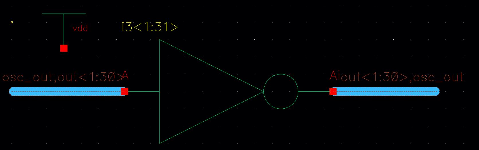
The input of I3<1> is osc_out and its output is out<1>
The input of I3<2> is out<1> and its output is out<2>
The input of I3<3> is out<2> and its output is out<3>
The input of I3<31> is out<30> and its output is osc_out
The schematic is exactly the same as the one we drew earlier but
clearly nicer.
Re-simulating this ring oscillator gives the exact same results as seen
above.
When you check and save ignore the errors or add no connection terminals
like done in tutorial 2.
Save and close all cells.
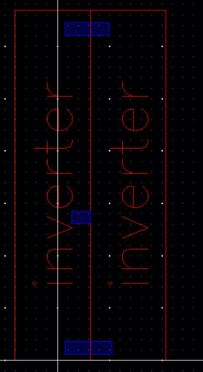
Create a new layout view for the ring oscillator. In its place two
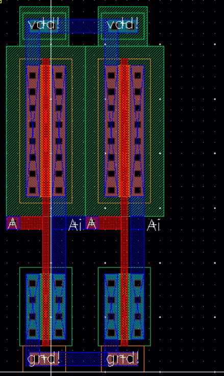
inverter cells next to each other, then save and DRC.
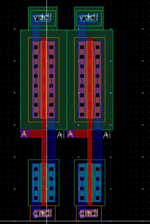
Add metal1 rectangles connecting the vdd! of the first inverter to the
vdd! of the second. Do the same thing for gnd!. Then with metal1
connect Ai of the first inverter to A of the second inverter.
Then DRC.
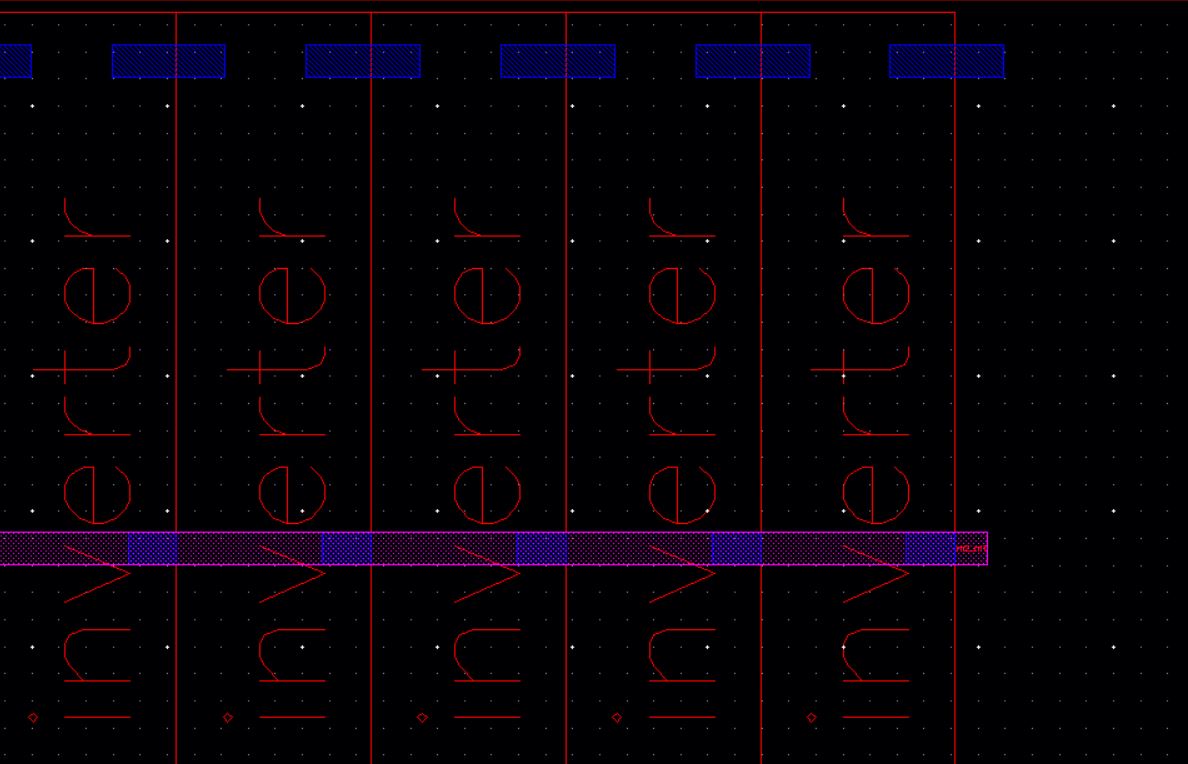
Next, delete the right inverter. Then select the entire layout
and press "c" to copy. Make 30 columns like before.
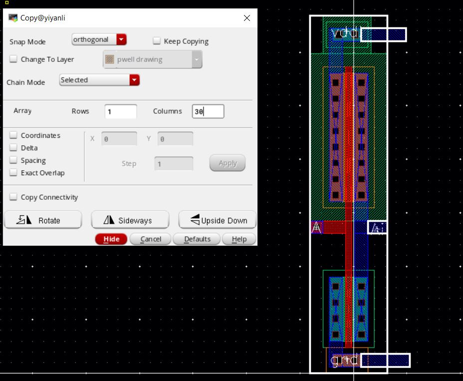
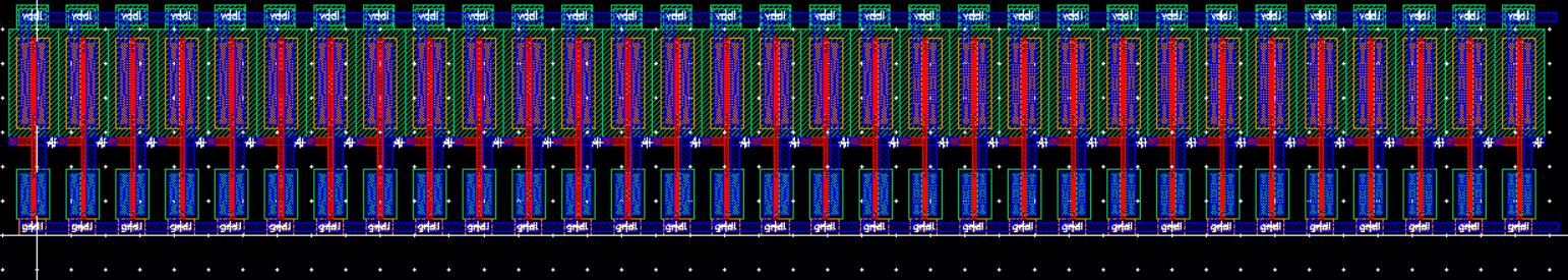
Place the inverters end-to-end as seen below. DRC the layout
Next add m2_m1 to the right and left sides of the layout as show.
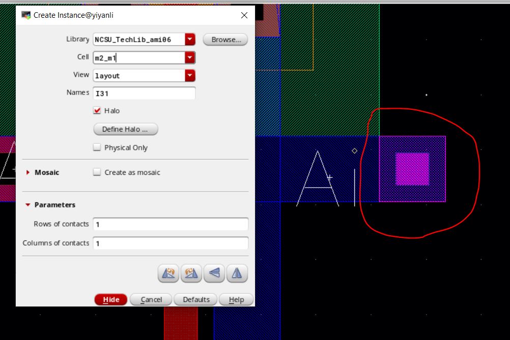
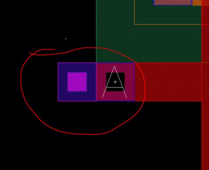
Now connect them using a metal2 rectangle. Below is the results
with stop display set to 0. DRC and save.
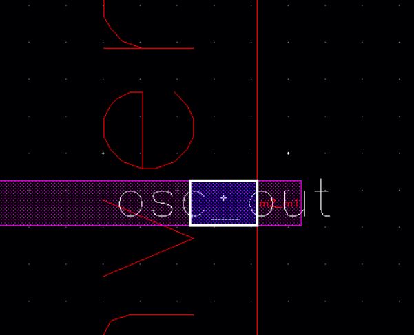
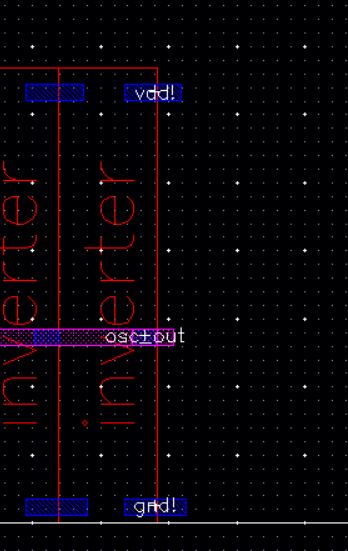
Next add vdd! (inputOutput), gnd! (inputOutput), and osc_out
pins (output). vdd! and gnd! will both be on meltal1. osc_out will
be on metal2. Place the pins as show below.
DRC, save then extract the layout. Save and close the layout
view; open the extracted view and run LVS.
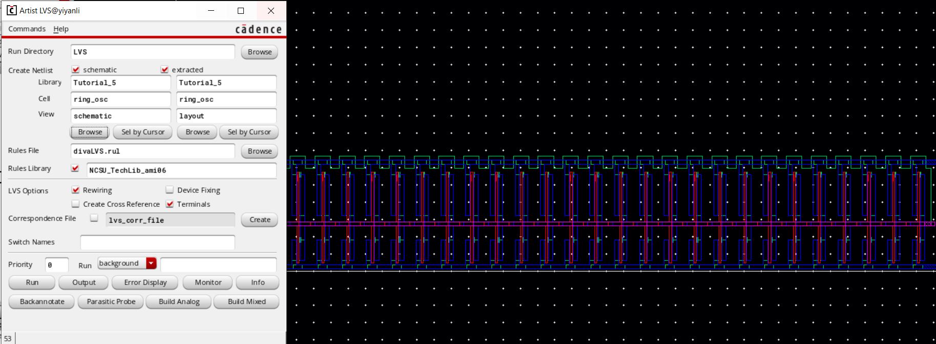
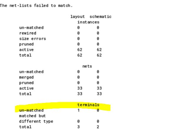
We see that the LVS failed. Why? Click on "Output" in the Artist
LVS window.
We can see that there is an unmatched pin.
We used a pin for osc_out in the layout but not in the schematic.
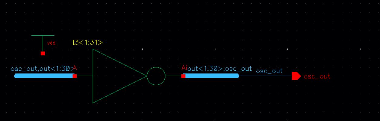
Let’s add a pin to the schematic. Make sure that the pin’s direction is
output.
Also note that the wire connection between the pin and the bus (wide
wire) must be labeled as seen.
When you are finished save and check, then close the schematic.
Re run the LVS and the netlist should match. If the LVS fails to
run restart cadence.
We now see that the netlists match.
Delete the vdd in the schematic
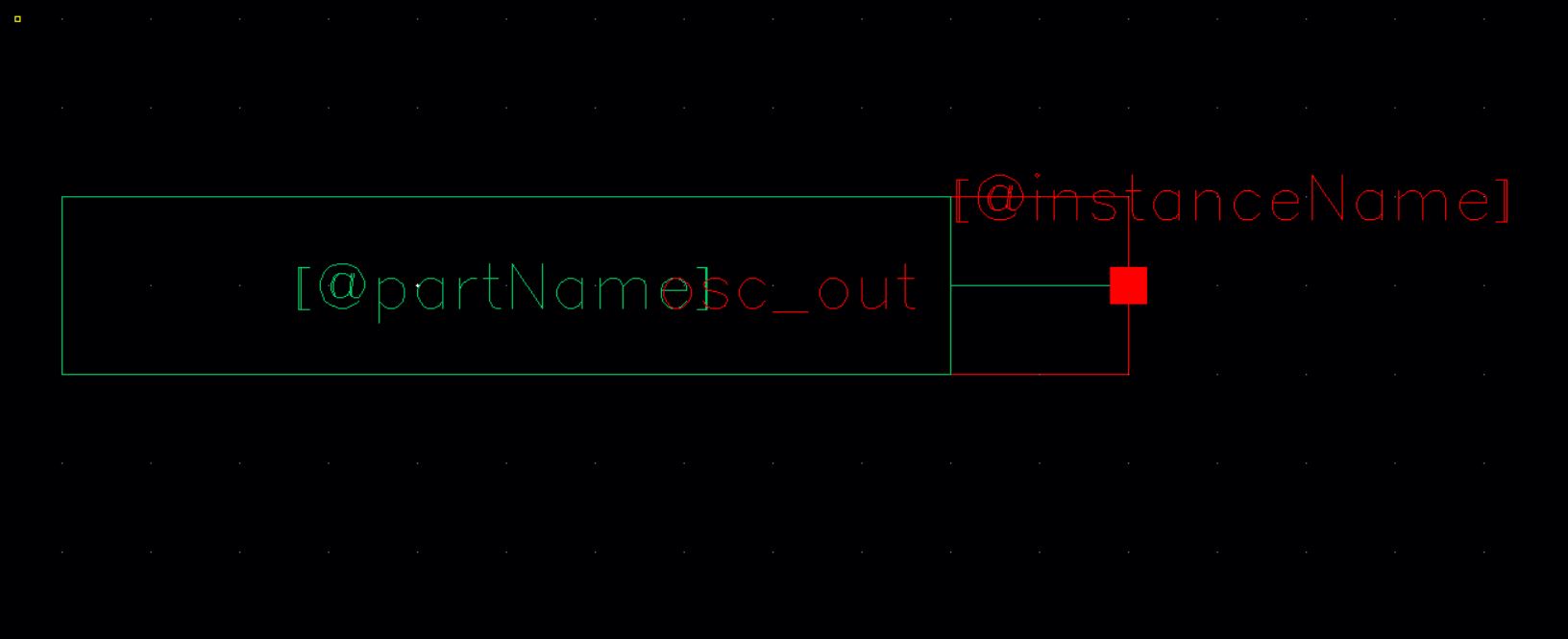
Create a symbol view for the ring oscillator.
Save and close all cell views.
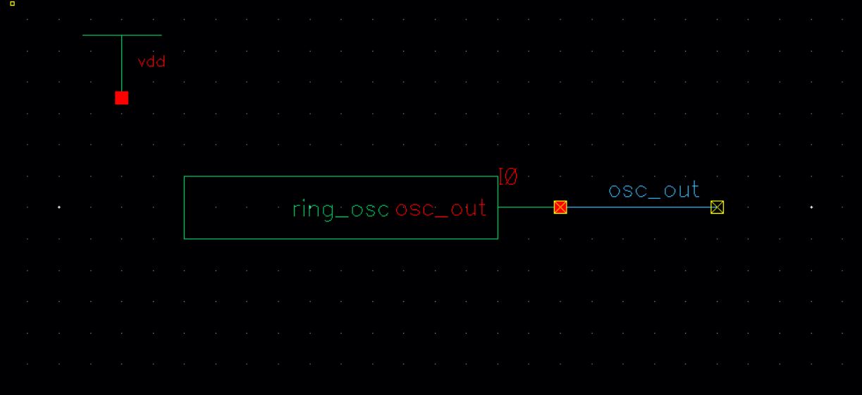
Create a new schematic cell view call sim_ring_osc.
Place the ring_osc and vdd symbols in this cell. Add a wire to
the output of the ring_osc symbol labeled osc_out as seen below.
Check and Save the schematic.
The two warnings are because of the floating wire. Ignore the
warnings like we have done in tutorial 1.
Launch ADE L and set up the simulation environment just like before.
Don't forget to set the initial condition.
When you are finished, save the state.
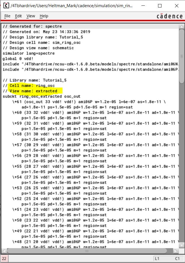
Now simulate the extracted view. To confirm that it used the extracted
view mouse over to "Simulations" then "Netlist" then "Display".
Confirm that the plot is the same. Do not save the state when
closing.
Congratulations you have finished tutorial 5. Continue to tutorial 6.