Tutorial
4: CMOS NAND gate
Start Mobaxterm and log on to
the Cadence server.
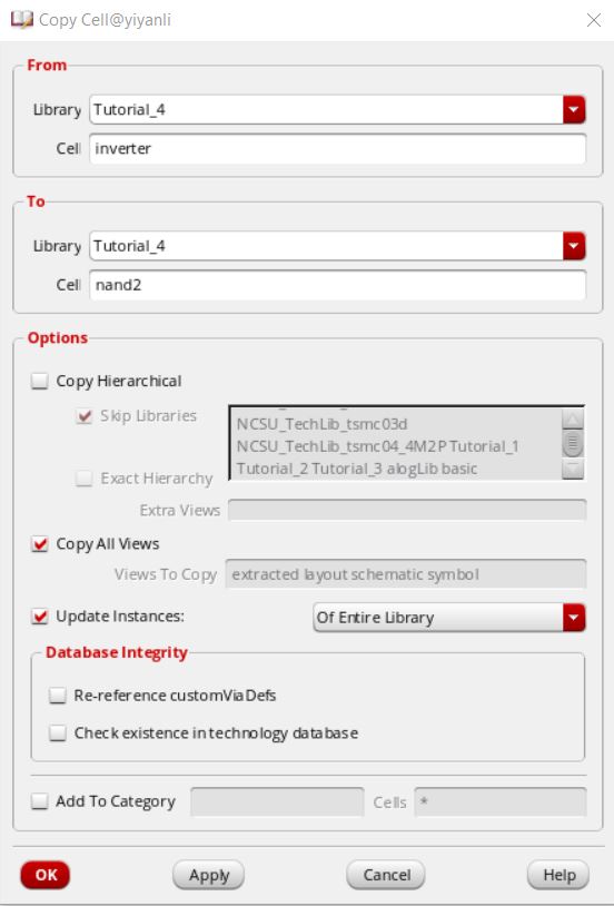
Copy the Tutorial_3 library into a new library called Tutorial_4.
Make sure that when you copy Tutorial_3 that the "update instances" box
is checked. Next
copy the inverter cell into a cell called nand2 (a 2-input NAND gate).
This is useful because now we do not have to remake the cells when we
are creating a new circuit layout.
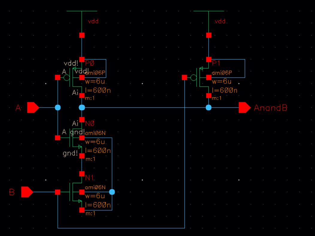
Open that NAND cell schematic and
create the circuit below. The pmos and nmos widths are now 6u. To
copy objects select the object that you want to copy then press "c", then click close to the object . Pin "B" is an input,
pin "AnandB" is an output.
Check
and save. The errors that appear are a result of the symbol not
matching the schematic. In the library manager delete the symbol view of the nand2 gate. This is a symbol
of the inverter.
Now check and save, there
should be no errors.
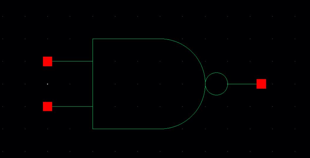
Next we are going to
create a symbol for the nand gate. Click "Yes" to overwrite sim info
and add/update inherited parameters.
Just like previously delete everything except for the pins and then draw
a NAND symbol (below). When you are finished check and save. Use the arc tool to draw the arc of the nand gate.
Now let's simulate the operation of the gate.
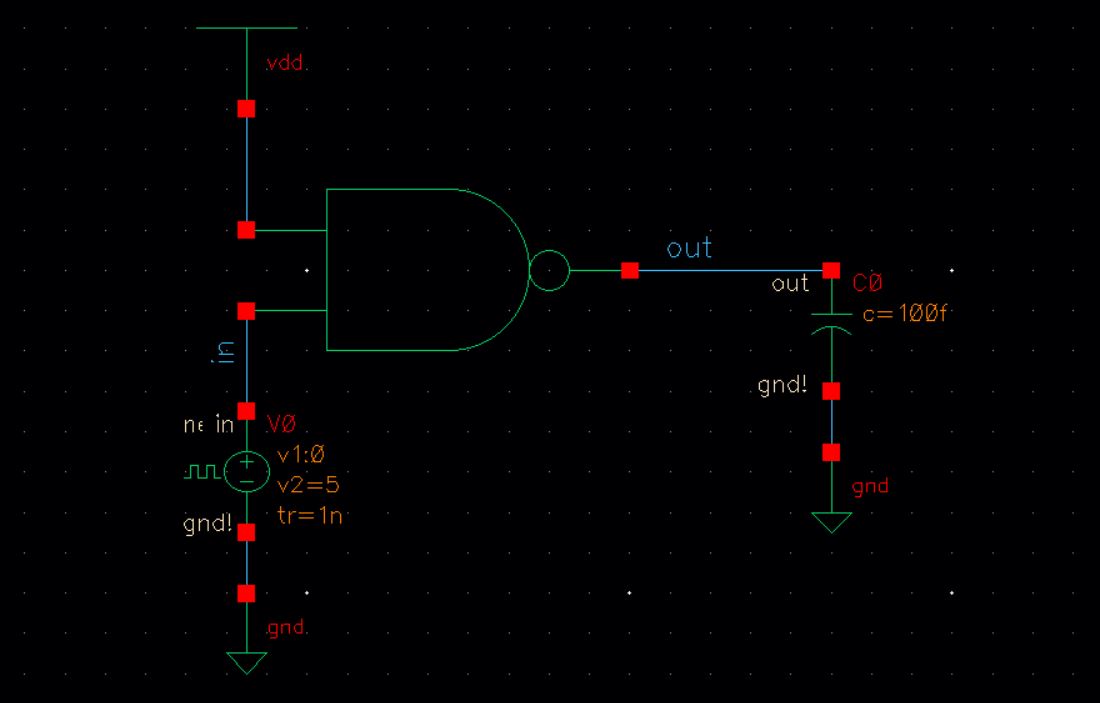
In the library manager create a new schematic cell called sim_nand2_tran.
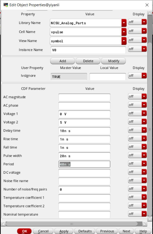
Create the following
schematic. Use a vpulse instead of a vdc. We also need a cap and
gnd. The cap is from the NSCU Ananlog Parts library - 'cap'.
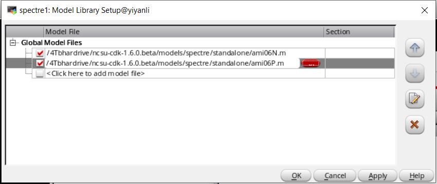
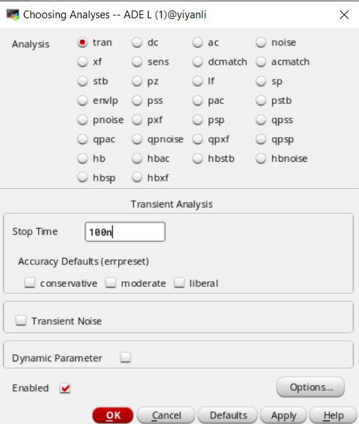
Next, open ADE L and set up the model libraries. You need both ami0P.m (pmos)
and ami0N.m (nmos).
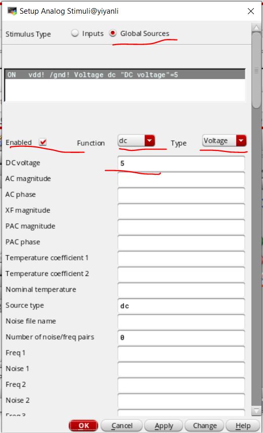
Set the vdd! to 5 V by setting up the "stimuli" under "setup". Make
sure that it is on Global Sources and "Enabled" is checked.
The outputs that will be save and plotted are the "in" and
"out" wires.
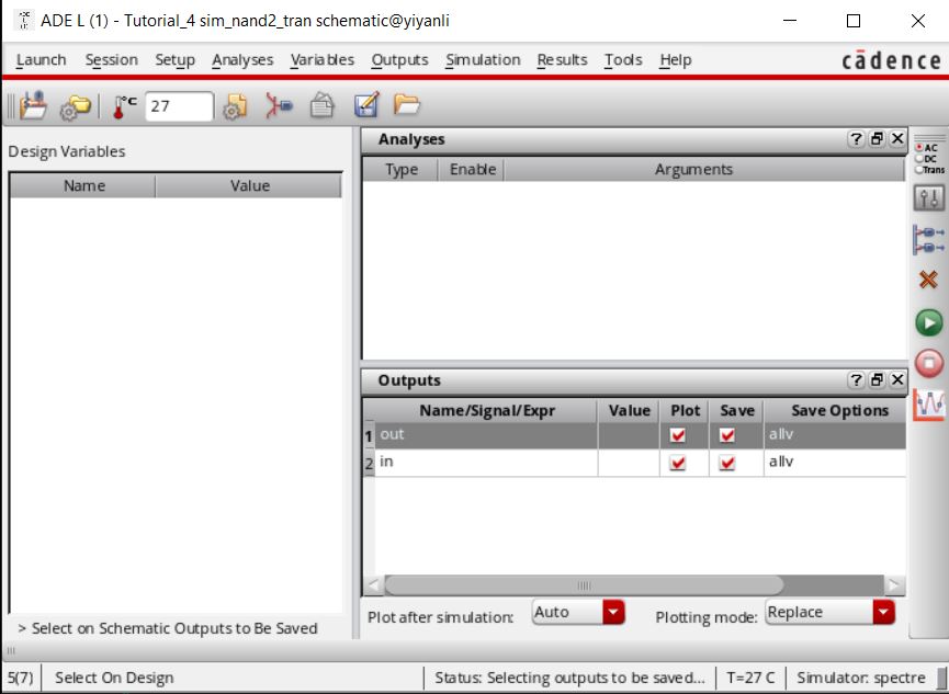
Finally, set the analysis to tran, then save the state as a cellview.
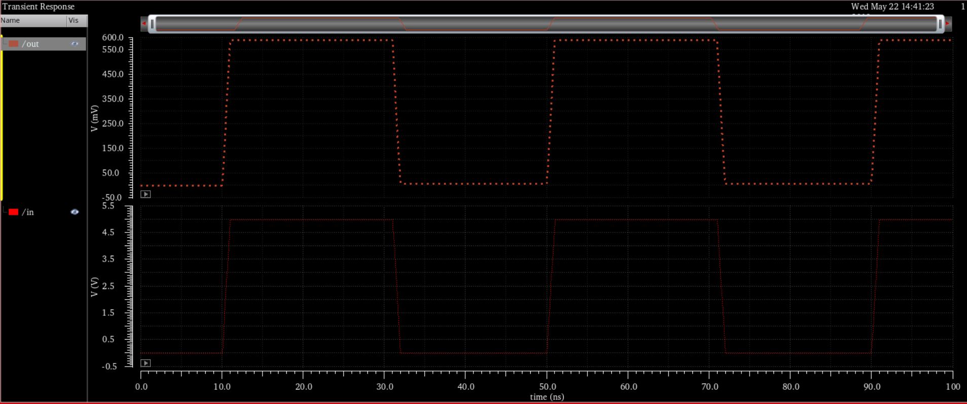
In the plot window spilt the graphs.
The two plot should look like the image below.
Save and close all open cell views.
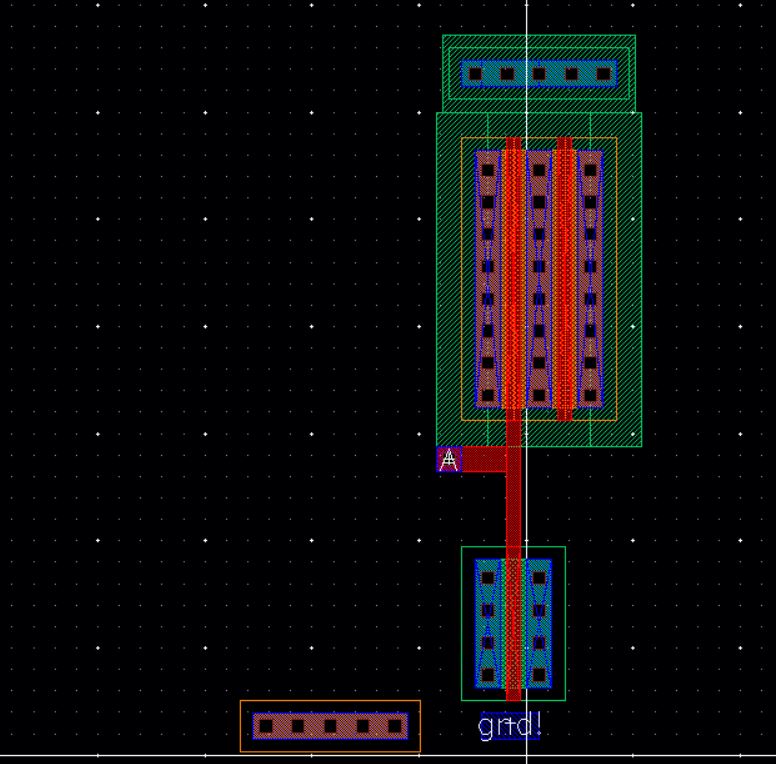
Open the nand cell layout from the library manager.
Delete the metal1 and "Ai" pin connecting the pmos and the nmos
together.
Then delete the metlal1 connecting the nmos to the ptap.
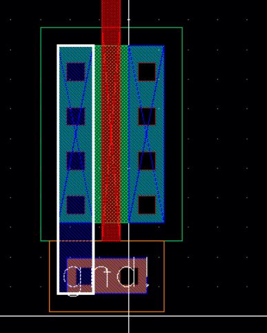
Then move the ptap over to the left side. Save and DRC. Fix any
errors.
Next delete the metal1 from the ntap to the left side of the PMOS and
delete the "vdd!" pin. Also delete the "gnd!" pin
Then copy the pmos cell.
Move the new pmos cell so that is overlapping the original pmos.
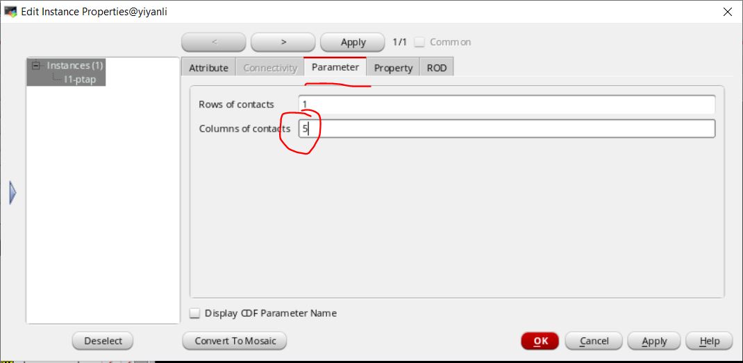
Then change the number of contacts in the ptap and ntap to 5. Save then
DRC.
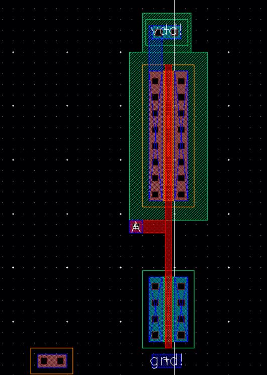
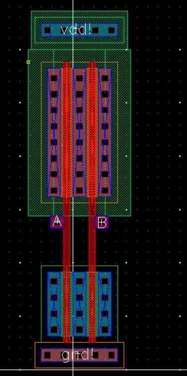
Now let’s make a copy nmos and overlap it with the first, like we
did above for the PMOS.
Let’s also move the m1_poly and A pin over adjacent to the vertical
poly and add a poly rectangle, m1_poly, and B pin (input) for the added
PMOS.
Ensure that pin names are showing, the pins are added on metal1.
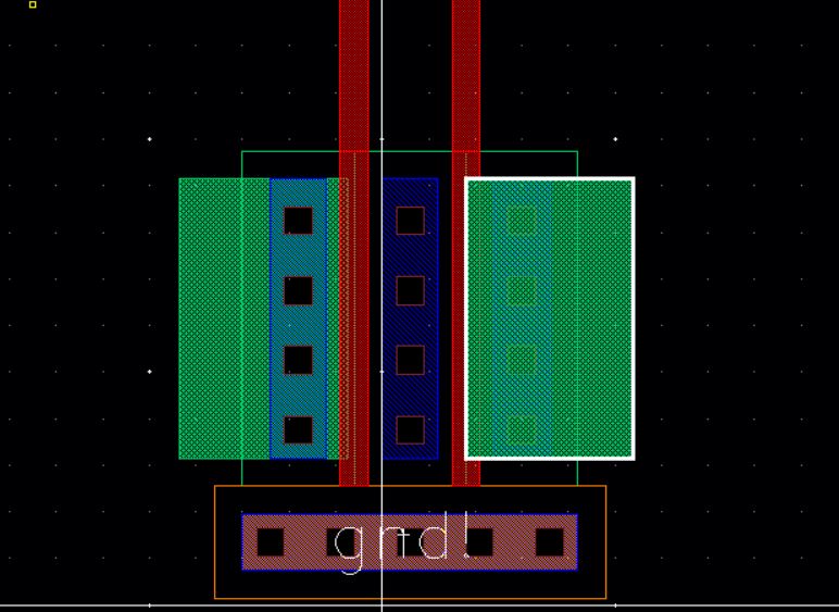
Now add add inputOutput pins for vdd! and gnd!
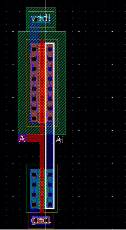
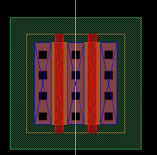
The result is seen below.
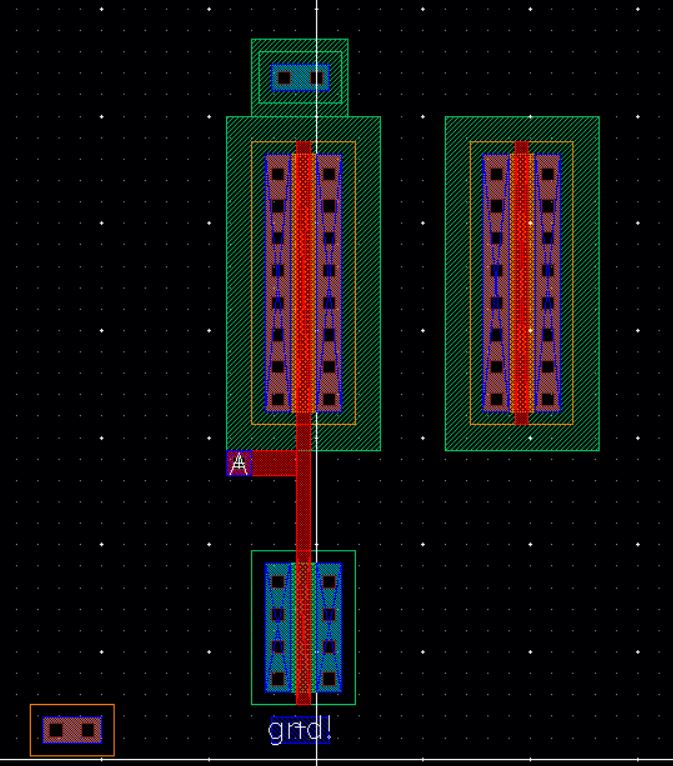
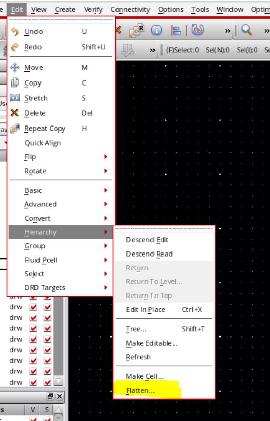
We now need to make it so there is not metal between the two
nmos. To do this we will flatten the hierarchies. With
both nmoses selected, click on "Edit" then to "Hierarchy" then click
on "Flatten".
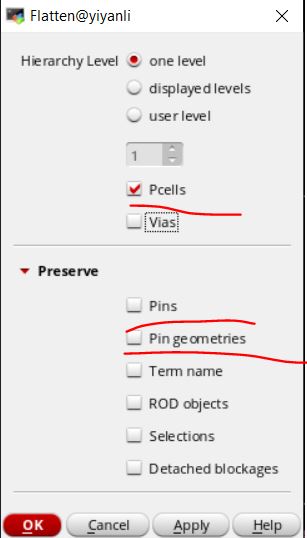
In the pop up window under the "Preserve" drop down deselect " Pins"
and " Pin geometries" . Then click "Ok".
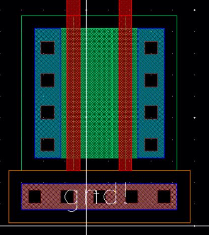
Now delete the metal in-between the two nmos. To do this you will
have to move some things around.
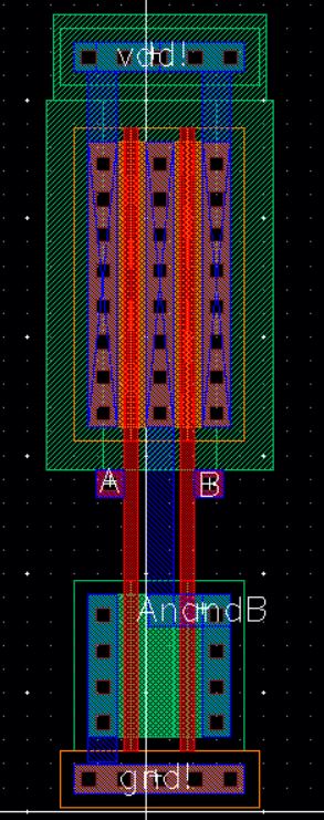
It should look as below when it is reassembled.
An alternative way to do this for the nmos is to set it up as two 'fingers'.
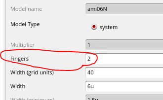
For the pmos, you can set the multiplier parameter to '2':
Add metal1 to gnd!, vdd!. Connect the drains of the two pmos to
the drain of the nmos. Finally add pin "AnandB" output as seen. DRC and
save.
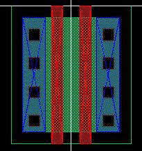
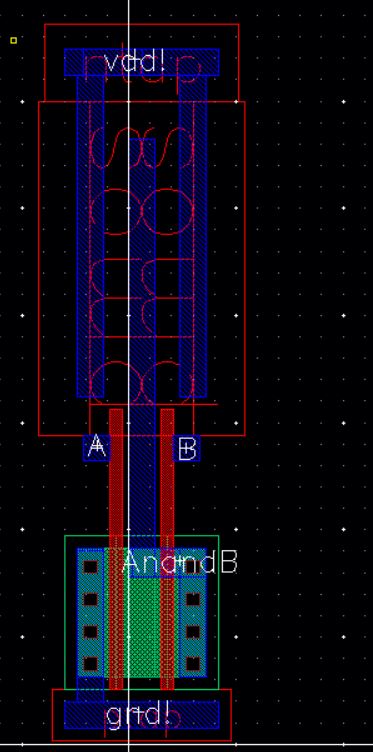
With the stop level set to 0 we get...
Extract the layout and open the extracted view with the Library Manager.
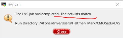
Run LVS.
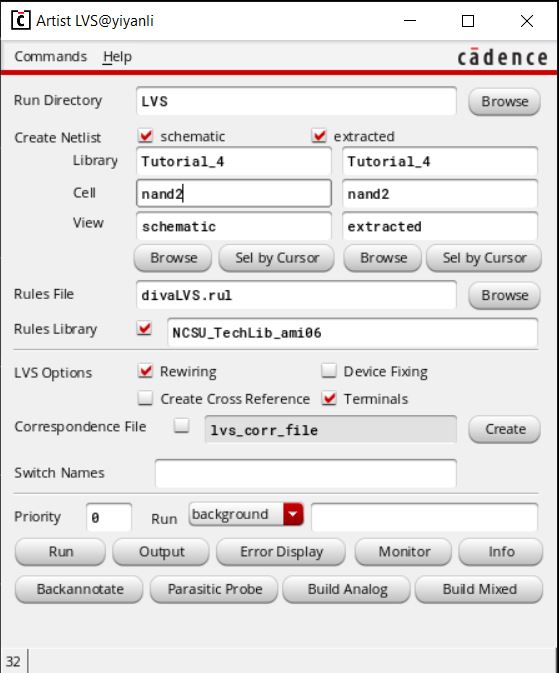
Make sure the layout and schematic match.
Congratulations You have finished Tutorial 4. Continue to tutorial 5