Tutorial
3: Inverter
Start Mobaxterm and log on
to the Cadence sever.
Create a new library called "Tutorial_3". Make sure you use the same
technology library as last time. .
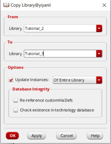
Copy everything in Tutorial_2 into Tutorial_3. To do this right click
on Tutorial_2 and click on copy. In the pop up window set the “to”
library to Tutorial_3 under options make sure that "Update
Instances" is checked. Then press "Ok".
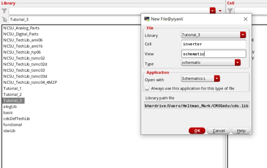
Next, in Tutorial_3 create a schematic Cell called inverter.
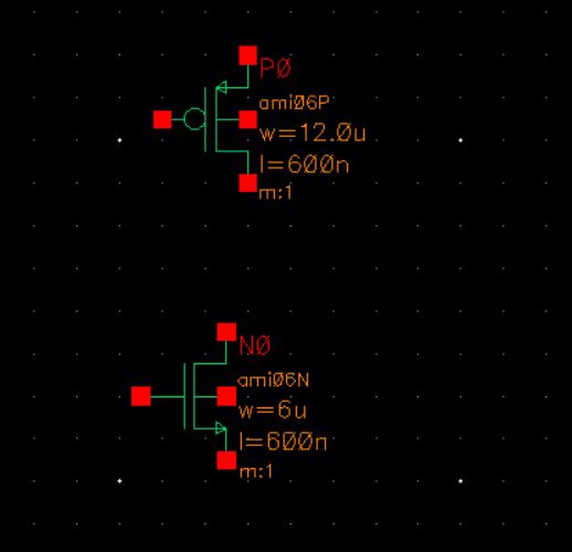
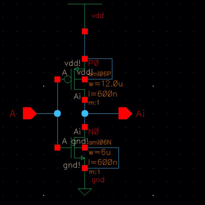
In the schematic place a pmos4 and an nmos4. The pmos has a width
of 12u and the nmos has a width of 6u.
Instead of using a vdc as our source of power we will use a vdd. In
the schematic place a vdd and a gnd from the NCSU Analog Parts Library.
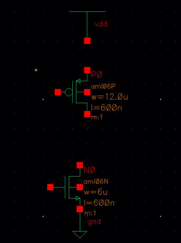
Finally, wire up the inverter
and add pins like below. The "A" pin should have an "input" direction
and
pin "Ai" should have an "output" direction. When you are finished check
and
save.
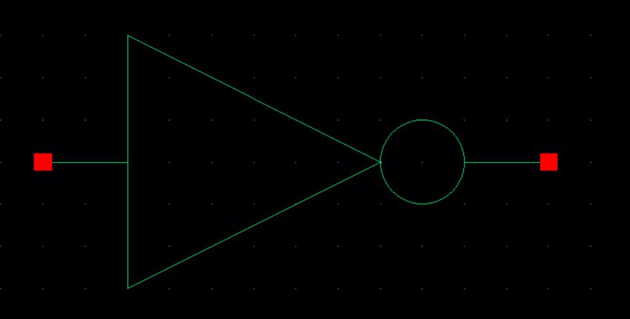
Next, create a new cell view
from the current cell view. This will be the symbol for the
inverter. To do this mouse
over to "Create" then to "Cellview" then to "From Cellview".
Press
"ok" on the first window. In the second window press "ok ".
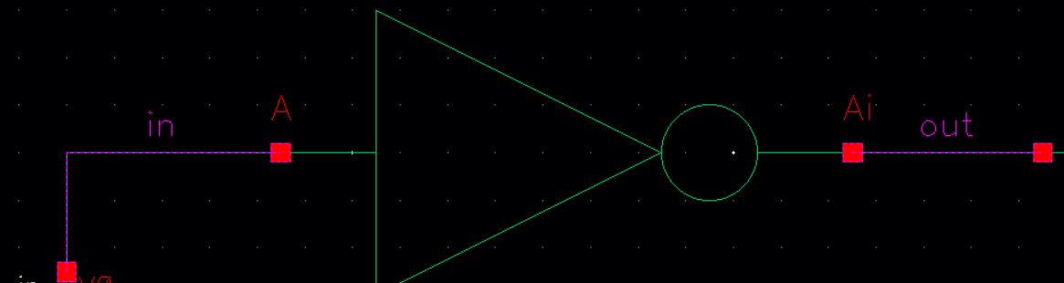
In the symbol view delete everything except the pins. Then,
draw the inverter symbol (see below).
Select
both pins then press "q" to edit their properties. Change "Apply to" to
"all
selected". Then change the "Display" to "value". Then press "ok".
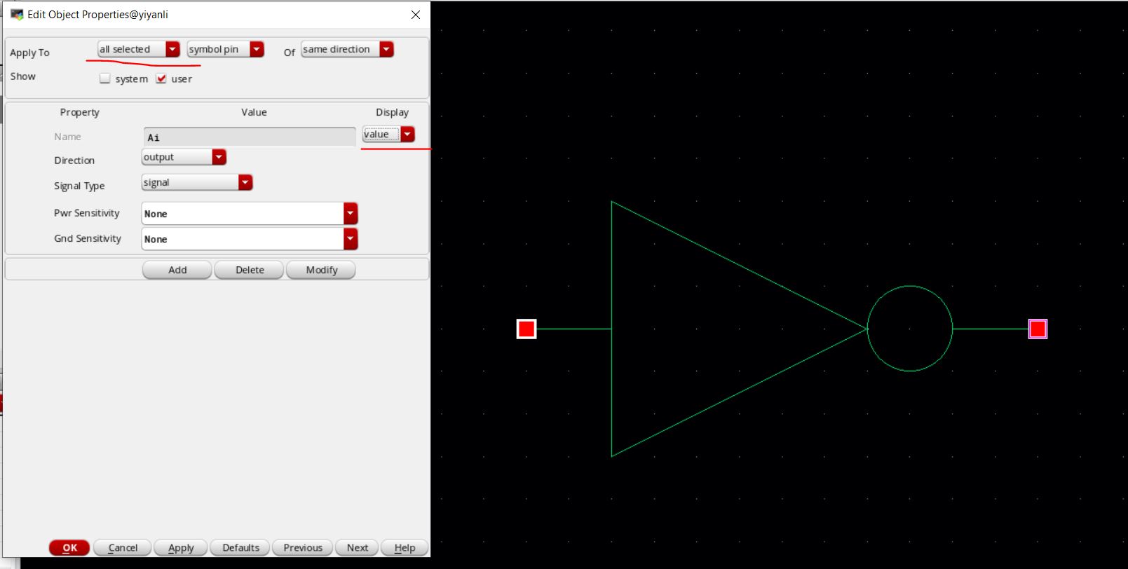
Check and Save.
We are now going to create the layout for the
inverter.
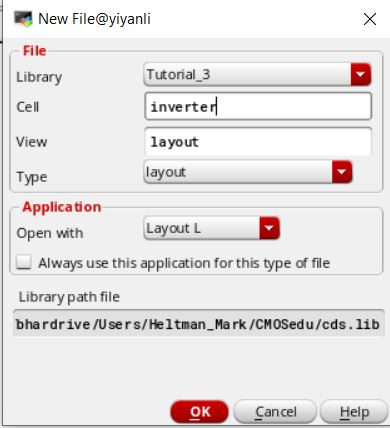
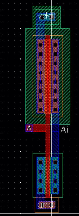
In the library manager create a new layout cell in Tutorial_3.
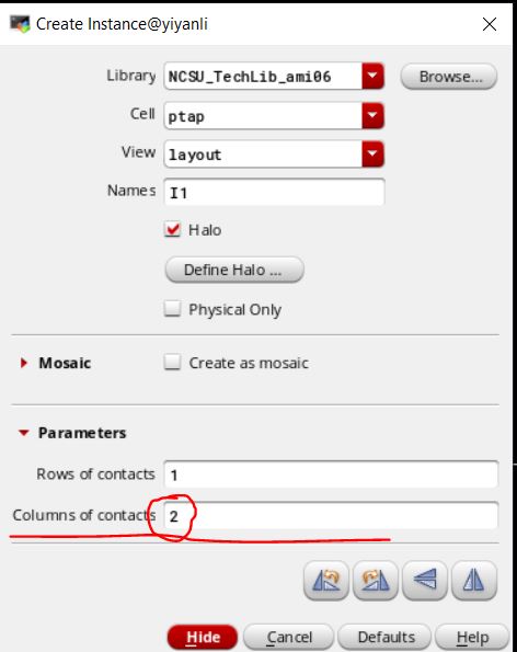
In the layout we need to add the following parts :nmos, pmos, ntap,
ptap, and m1_poly. Make sure that the nmos has a width of
6u and the pmos has a width of 12u. The ntap and ptap will use 2
columns of contacts.
Save and DRC. Fix any errors that come up.
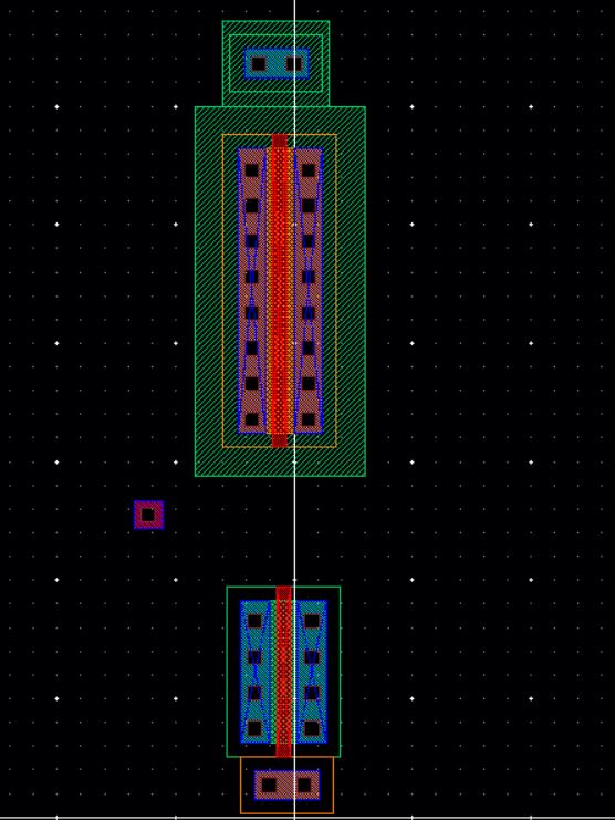
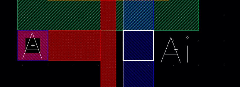
Add metal1 and poly rectangles as shown below. The metal1
rectangles will not align perfectly with the ntap and ptap contacts.
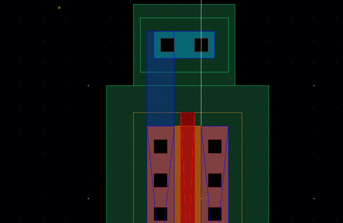
Save then DRC Fix any errors that occur.
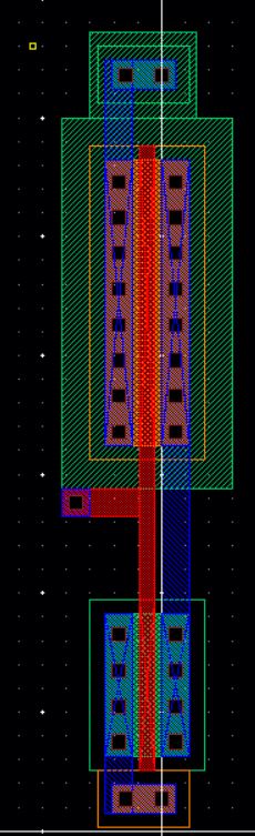
Next add pins on metal1 for gnd!, vdd! (Both have a direction of
inputOutput), A (input), and Ai (output). Make sure create label is
checked.
Next extract the layout and open it.
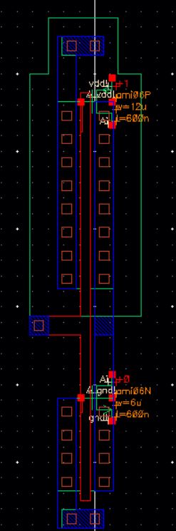
Now run an LVS.
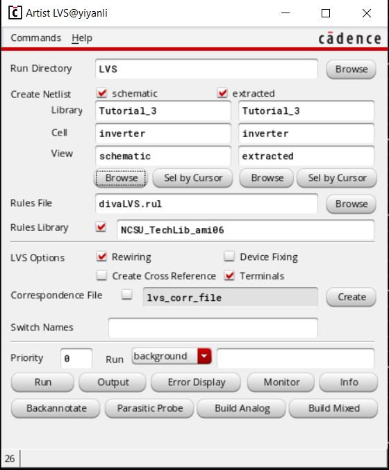
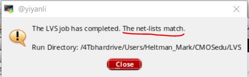
If the LVS succeeded then continue on. If it did not fix the errors
until it does succeeded.
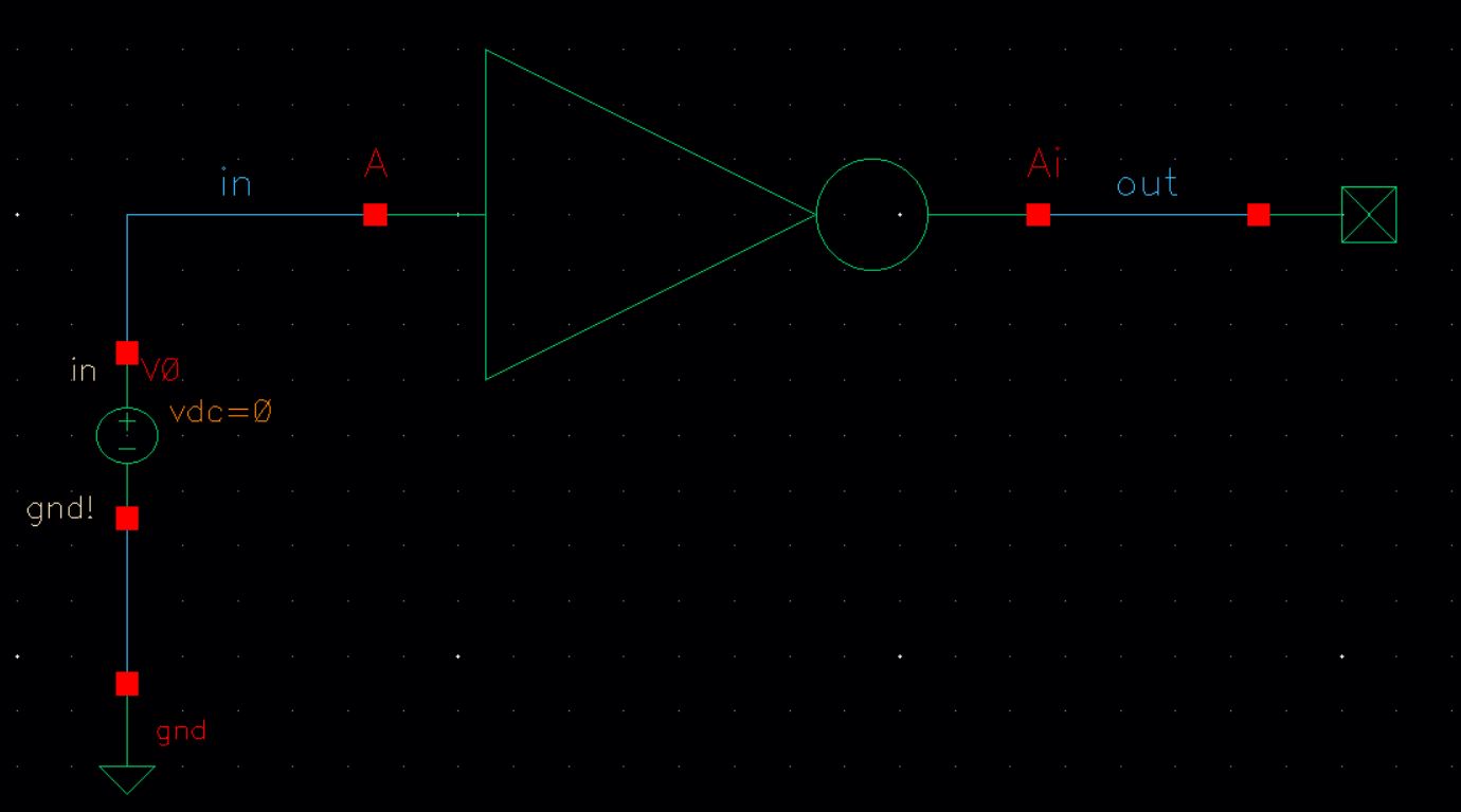
We are now ready to simulate. Create a new schematic cell in
Tutorial_3 called "sim_inverter_dc".
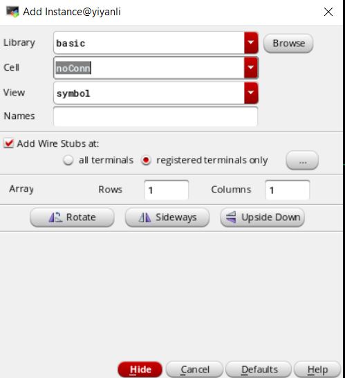
Draw the following schematic. The symbol on the right of the "out" wire
is the "no-connection" symbol. We add the symbol so that we can avoid
the floating pin/nets warnings that we got in the first tutorial.
When you are finished save and check, then, fix any errors.
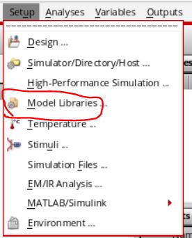
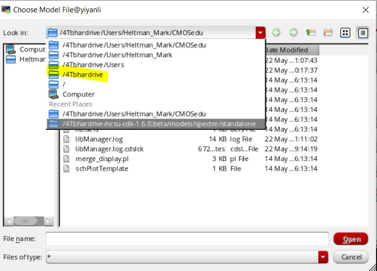
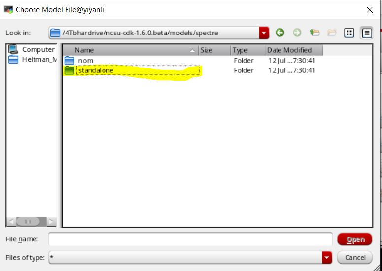
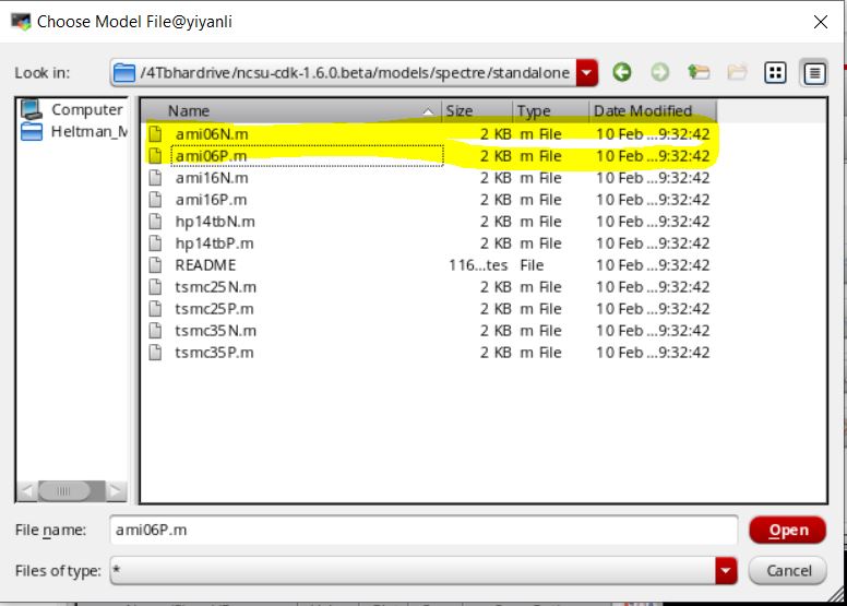
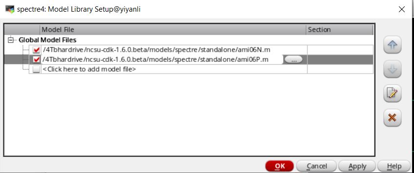
Start ADE L then select the model
files ami06N.m (nmos) and ami06P.m (pmos).
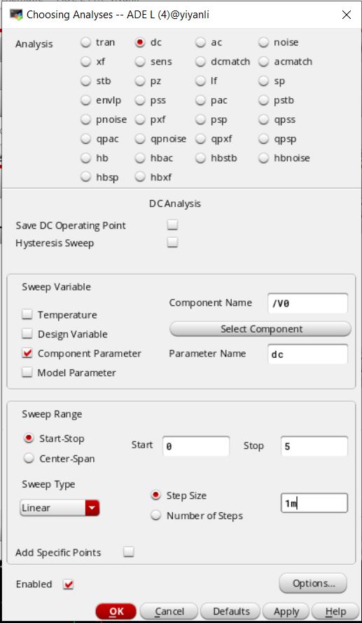
Set the Analyses to whats seen below.
Next, the outputs that we want to save and plot are wires "in" and
"out".
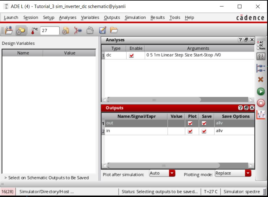
Save the state as a cellview.
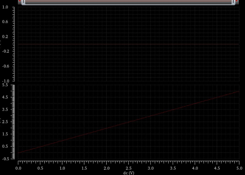
Press the green button( ) to start the analysis. In the
plot click on
) to start the analysis. In the
plot click on  to spilt the plots into two separate graphs. We can see that the
output is zero. That is because we do not have power running to the
inverter.
to spilt the plots into two separate graphs. We can see that the
output is zero. That is because we do not have power running to the
inverter.
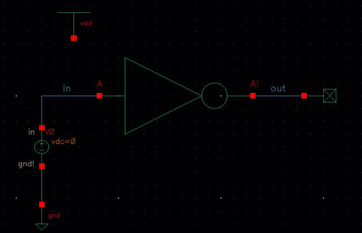
Add a vdd to the schematic. Check and save, fix any errors. Make
sure that you don't put the vdd to close to the inverter or you will
get an error.
Now we need to add the vdd to the simulation. Mouse over to
"Setup" then click on "Stimuli".
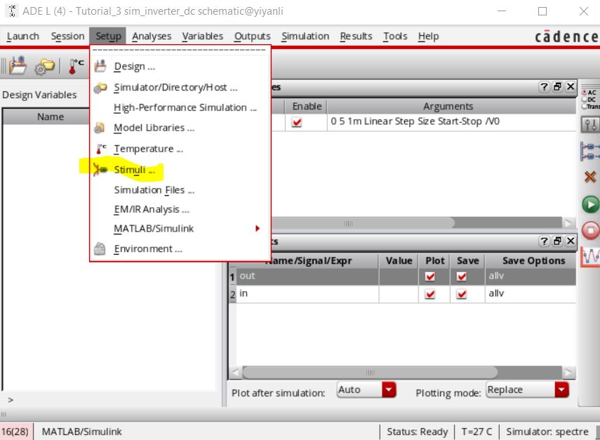
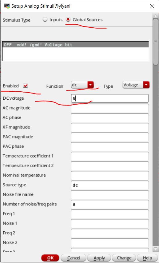
Click on "Global Sources".
Then set up the following parameters. When that is completed
click "Apply" then "ok"
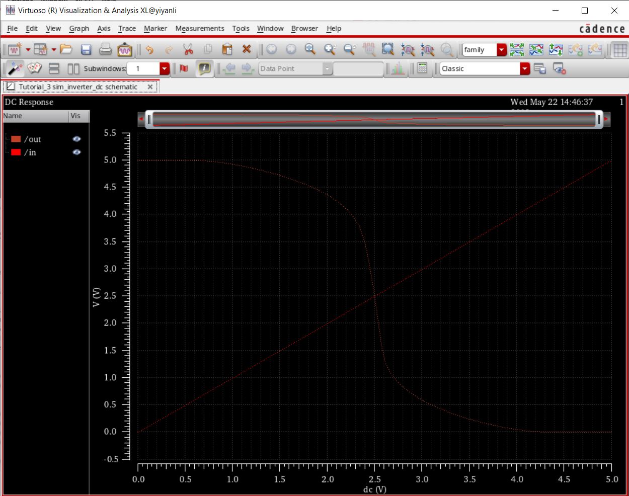
Save the state as a cell
view. Next, click
run and the pot should look like the one below.
Now simulate the extracted
view. Following the same steps as last time.
If your plots are the same,
Congratulations!!!!! You have finished tutorial 3. Do not save the current
state.
Move on tutorial 4.