Lab 2 - Verilog, Vivado, and FPGA Basics
Name: Taylor Schermer
Email: tschermer@fortlewis.edu
Task 1:
1. Go through all the steps in this
lab instruction, report your code, simulation results, and the on-board
verification results. (30 points)
Note: On-board verification shown in Task 3.
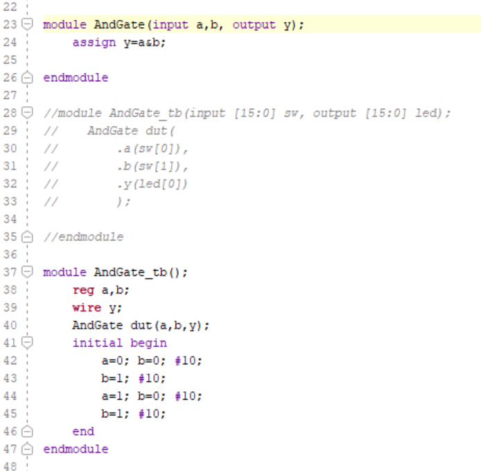
Figure 1. And Gate Code
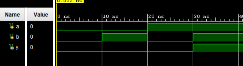
Figure 2. And Gate Simulation
As displayed in the simulation, my and gate logic works properly. Below in my demonstration of volatile and nonvolatile memory you can see it in action.
Task 2:
2. Use the same procedure to create
XOR and OR gates. Run simulations to verify the logic. (30 points)
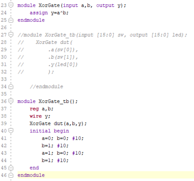
Figure 3. XOR Gate Code
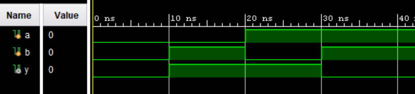
Figure 4. XOR Gate Simulation
As displayed in the simulation, my xor gate logic works properly.
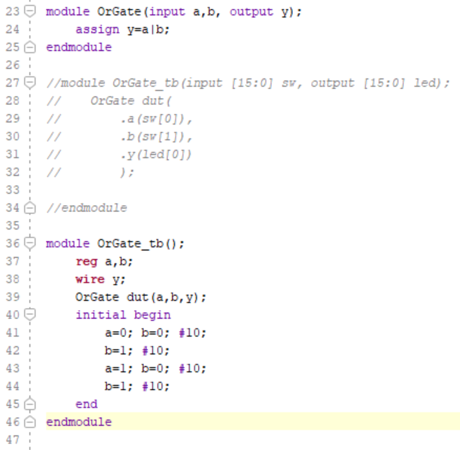
Figure 5. Or Gate Code
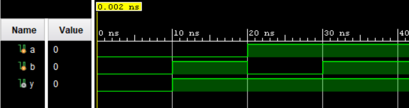
Figure 6. Or Gate Simulation
As displayed in the simulation, my or gate logic works properly.
Task 3:
3. Use both the volatile and
nonvolatile methods (QSPI) to program your FPGA. Show videos for the
demonstrations. (40 points)
As you can see in the video, non-volatile memory is still accesible even if power is cut from the device.
On the other hand, if power is shut off from the device volatile memory is lost.
What I learned:
In this lab we utilized vivado to
program an and gate, xor gate, and or gate and run simulations to verify
logic. We applied our and gate to our Basys3 to learn how connect our
hardware to our logic. We programmed to volatile memory to demonstrate
that when power is cut our logic is lost. We also programmed to
non-volatile memory to show that memory can be saved there when power is
cut.