ENGR336 Lab 2022 Fall
Lab 7:
Using Buses in Electric VLSI
Name: Seth VanMatre
Email: sgvanmatre@fortlewis.edu

Using Buses in Electric VLSI

Introduction

The objective of this lab is to layout and simulate a Ring Oscillator, 8-bit AND gate, 8-bit OR gate, 8-bit NAND gate, 8-bit NOR gate,      

Materials and Methods

- Electric VLSI

Results

Task 1:  Ring Oscillator
Task1_RingOscillator.png
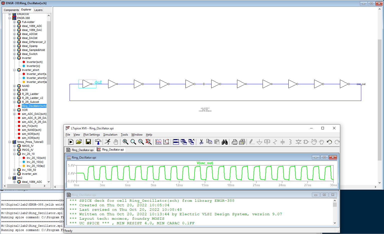
Figure 1: Ring Oscillator Schematic.

Task1_RingOscillator_Bus.png
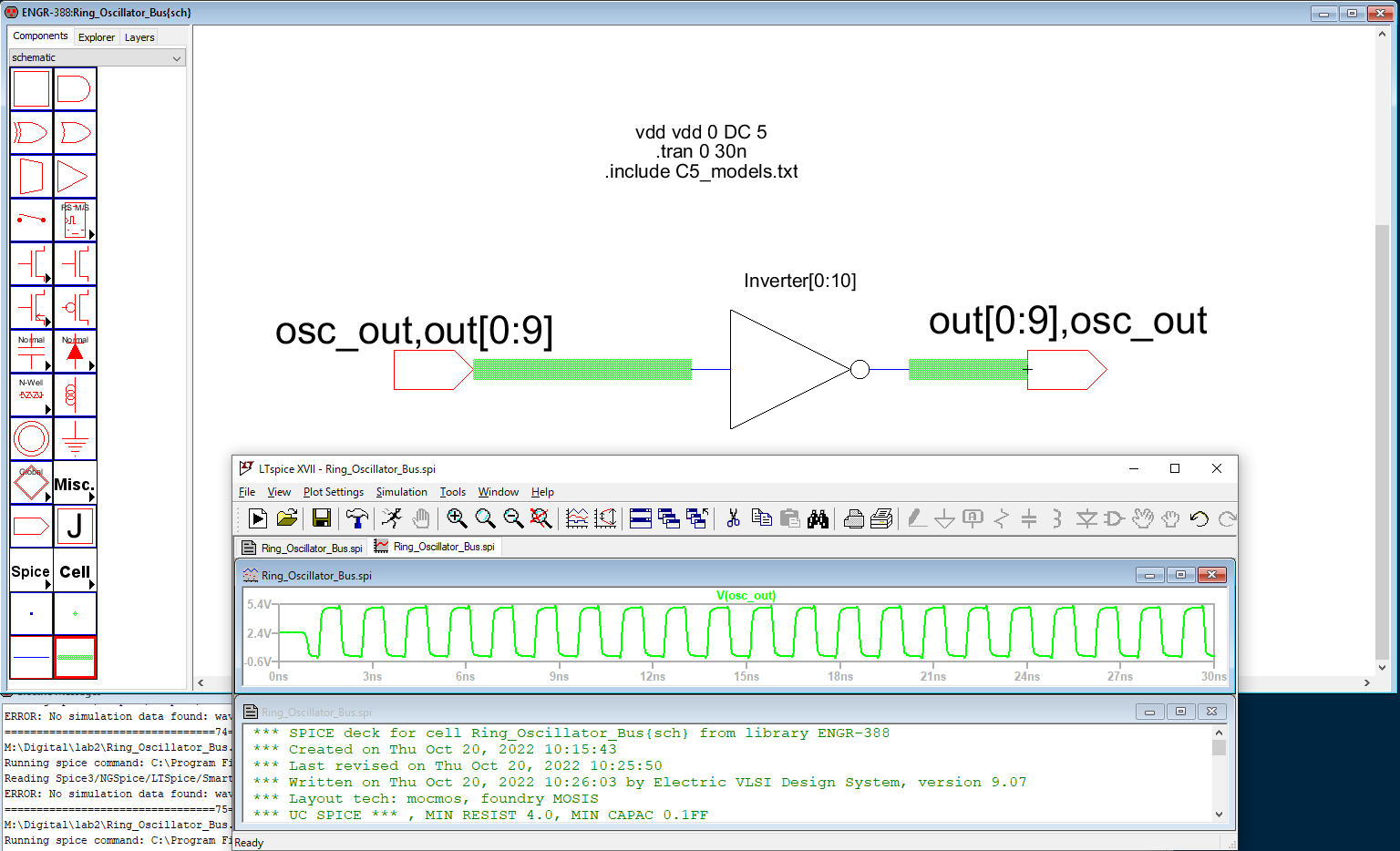
Figure 2: Ring Oscillator Bus Schematic.


Task1_RingOscillator_Bus_Layout.png
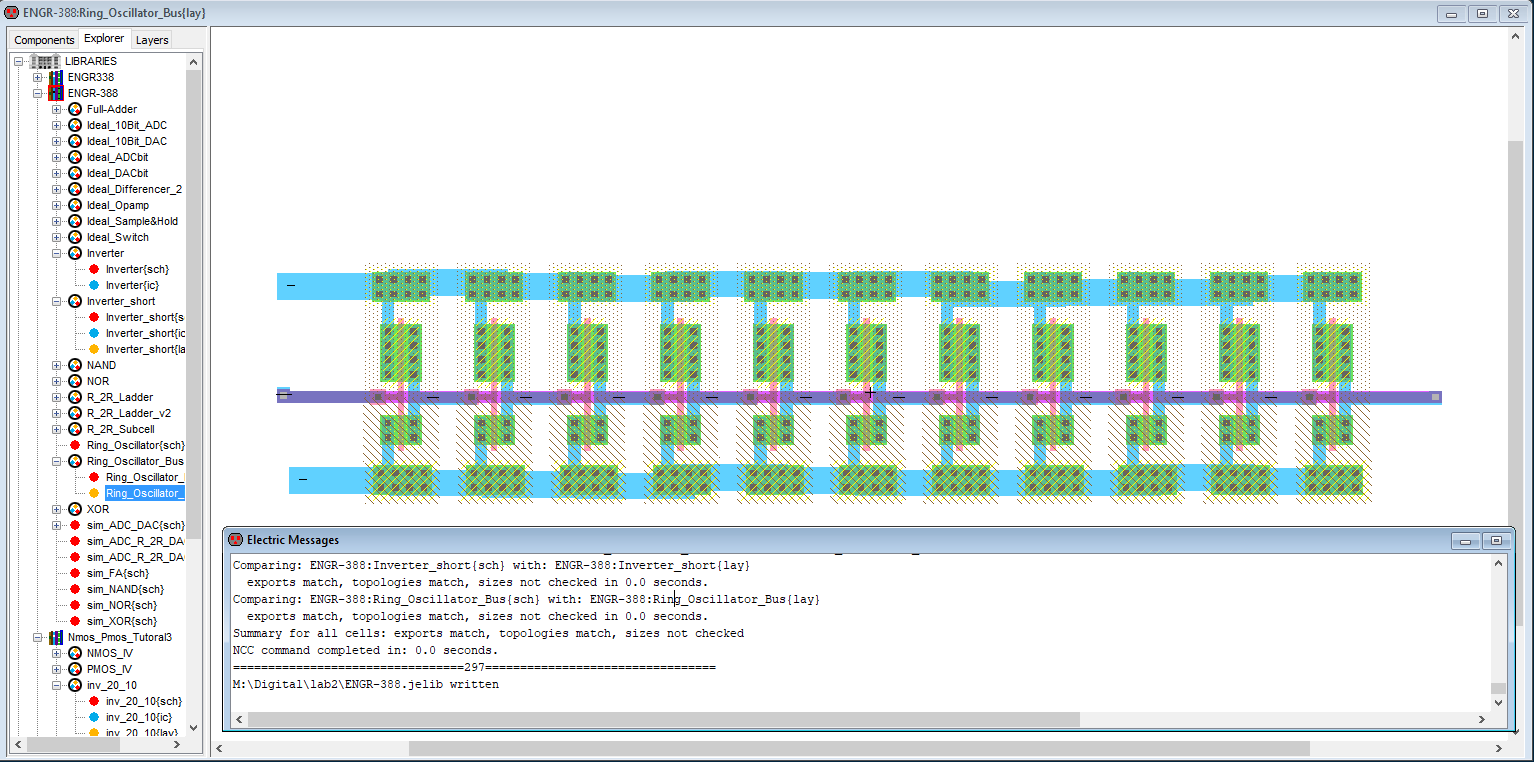
Figure 3: Ring Oscillator Bus Layout.


Task 2: 8-bit AND gate
Task2_AND-Schematic.png
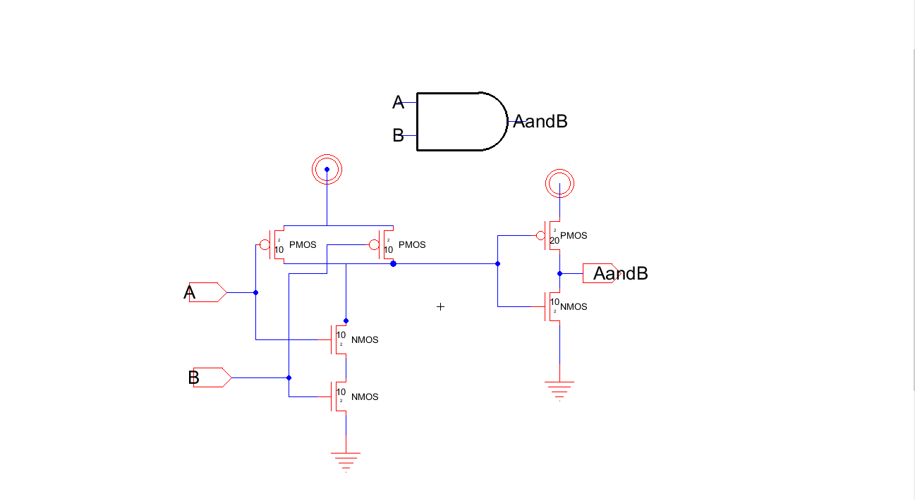
Figure 4: AND Schematic.


Task2_8-bitAND-GND.png
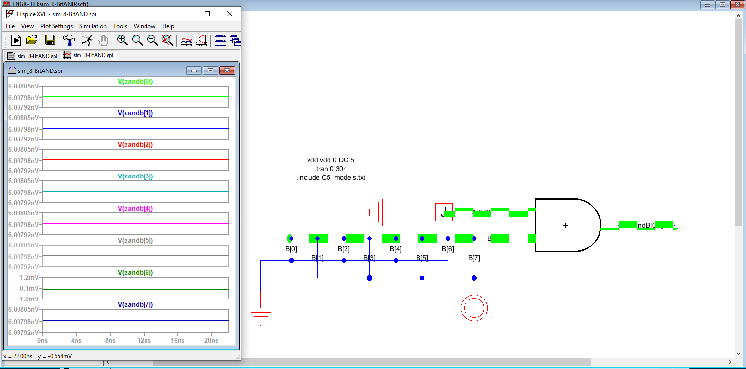
Figure 5: 8-Bit AND Voltage Source.


Task2_8-bitAND-GND.png
Figure 6: 8-Bit AND GND.


Task2_AND-Layout.png
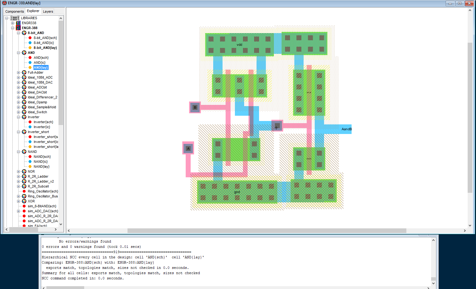
Figure 7: AND Layout.


Task2_8-bitAnd-Schematic.png
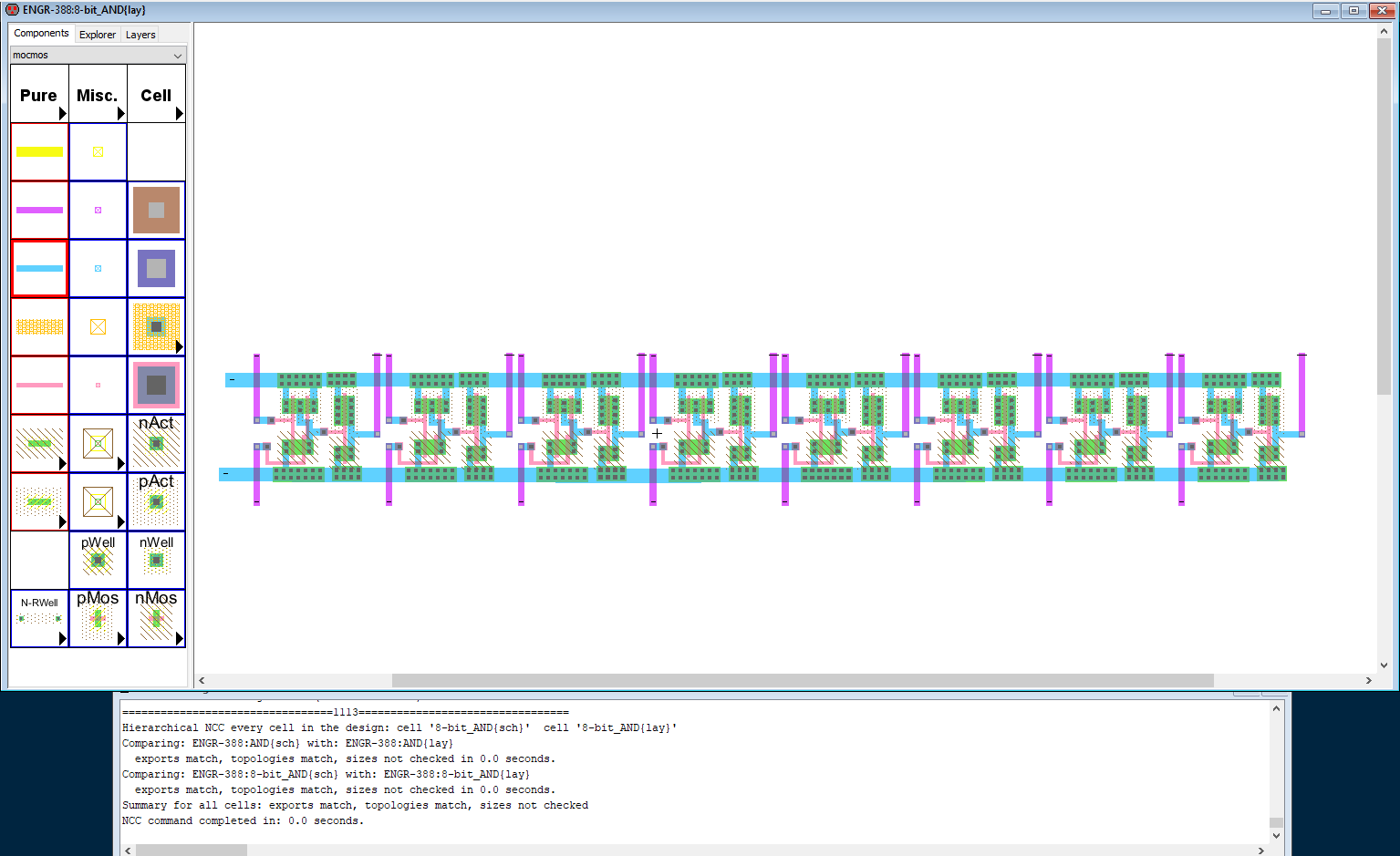
Figure 8: 8-Bit And Layout.


Task 3: 8-bit OR gate
Task3_OR-Schematic.png
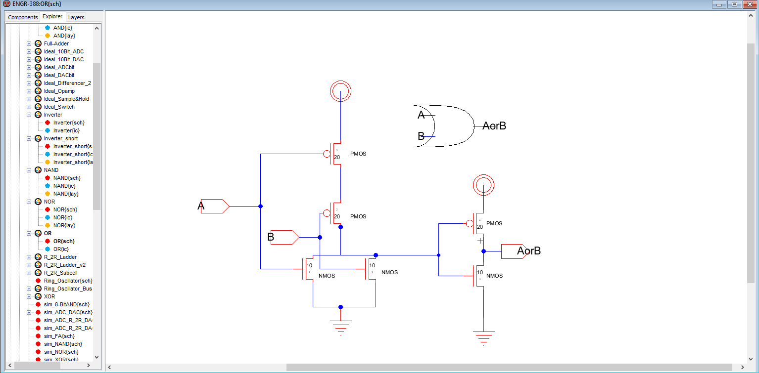
Figure 9: OR Schematic.


Task3_OR-Spice.png
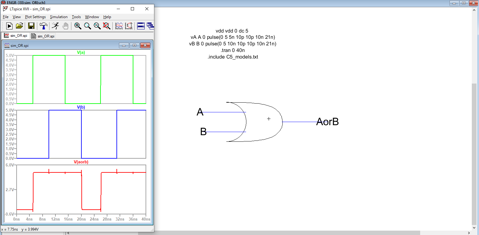
Figure 10: OR Spice Simulation.


Task3_OR-8Bit-Voltage.png
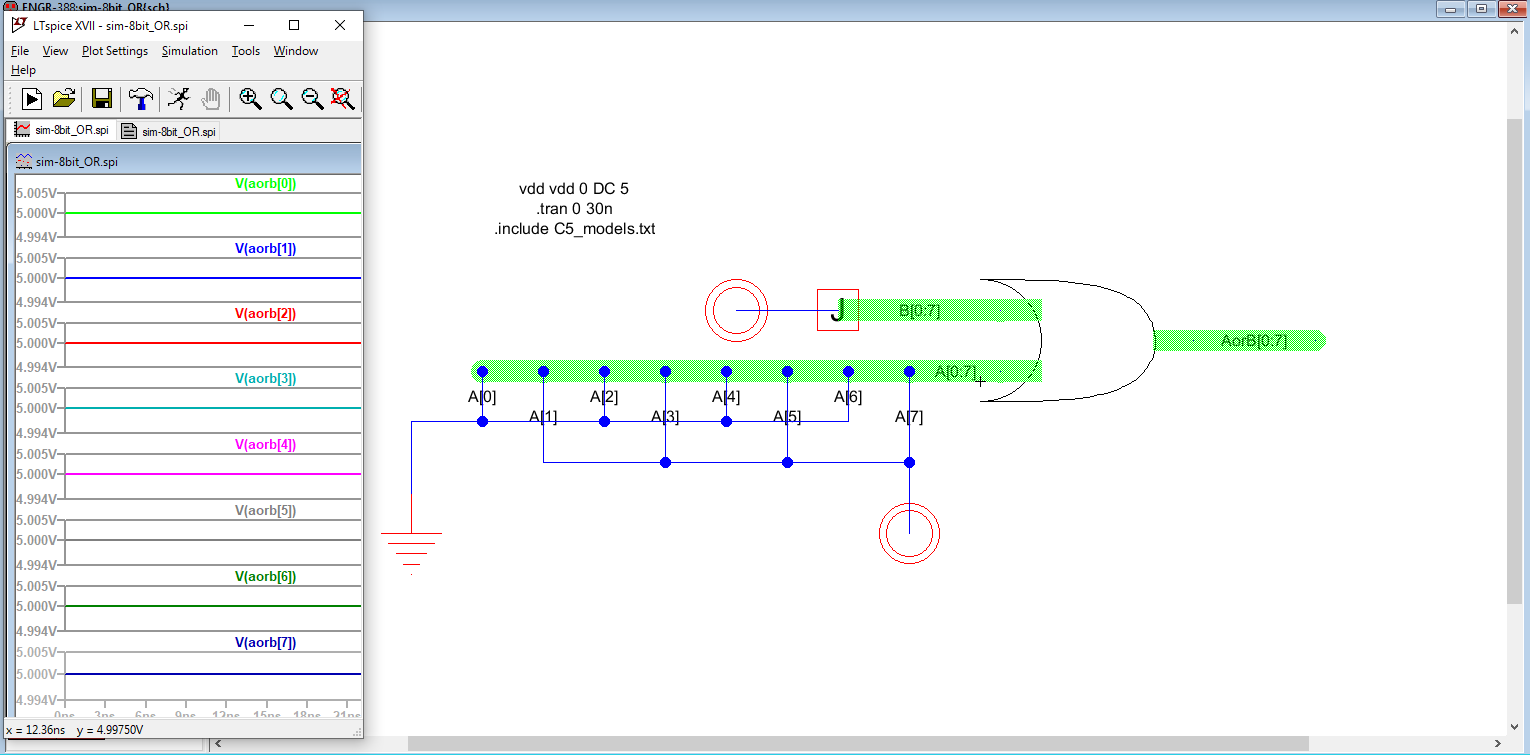
Figure 11: OR 8Bit Voltage Source.


Task3_OR-8Bit-GND.png
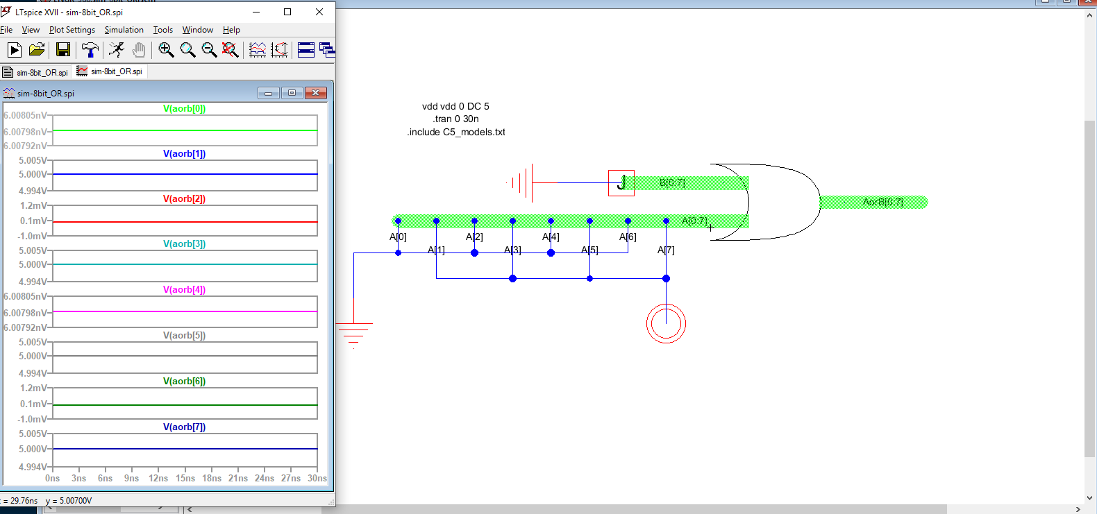
Figure 12: OR 8-Bit GND.


Task3_OR-Layout.png
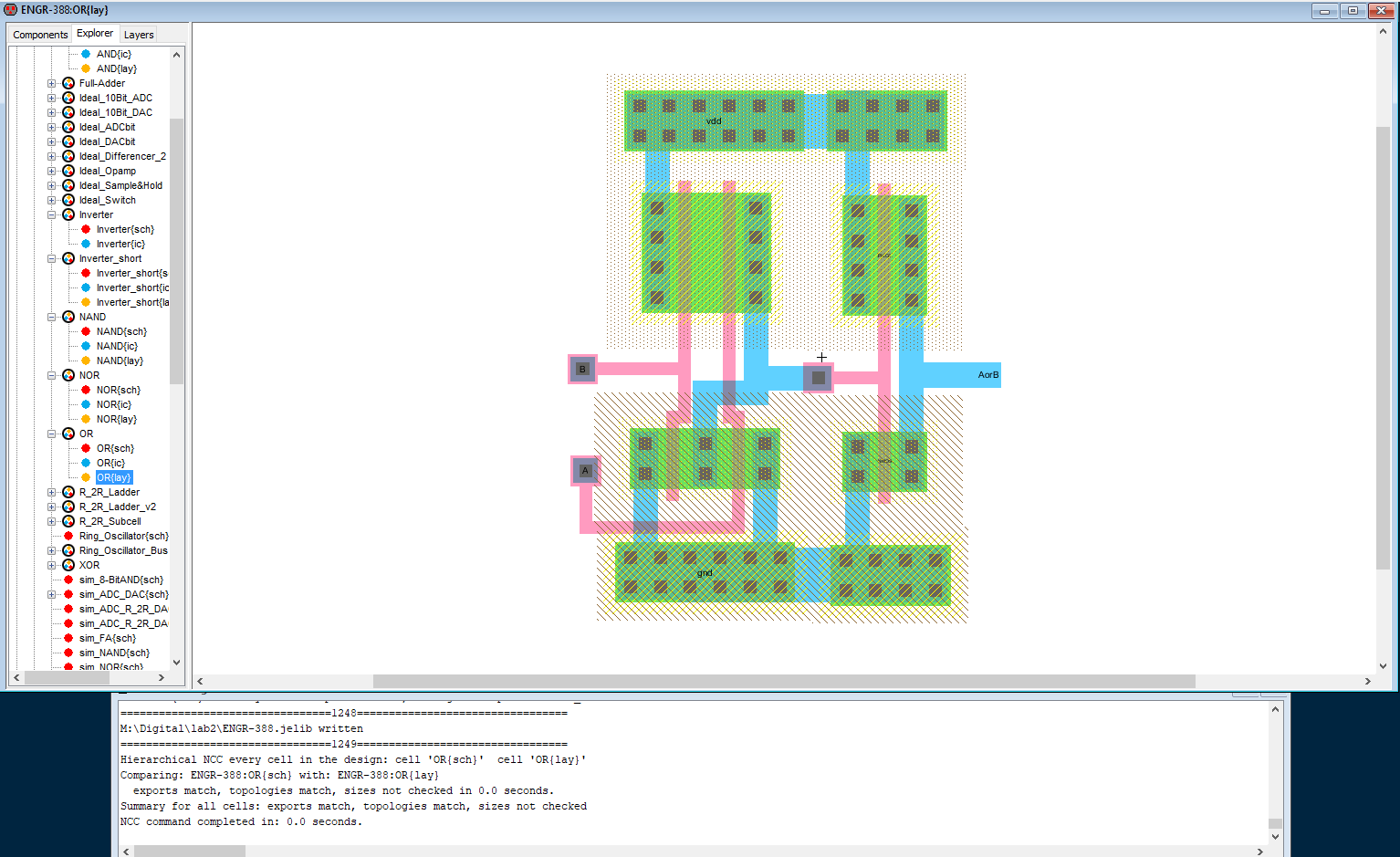
Figure 13: OR Layout.


Task3_OR-8Bit-Layout.png
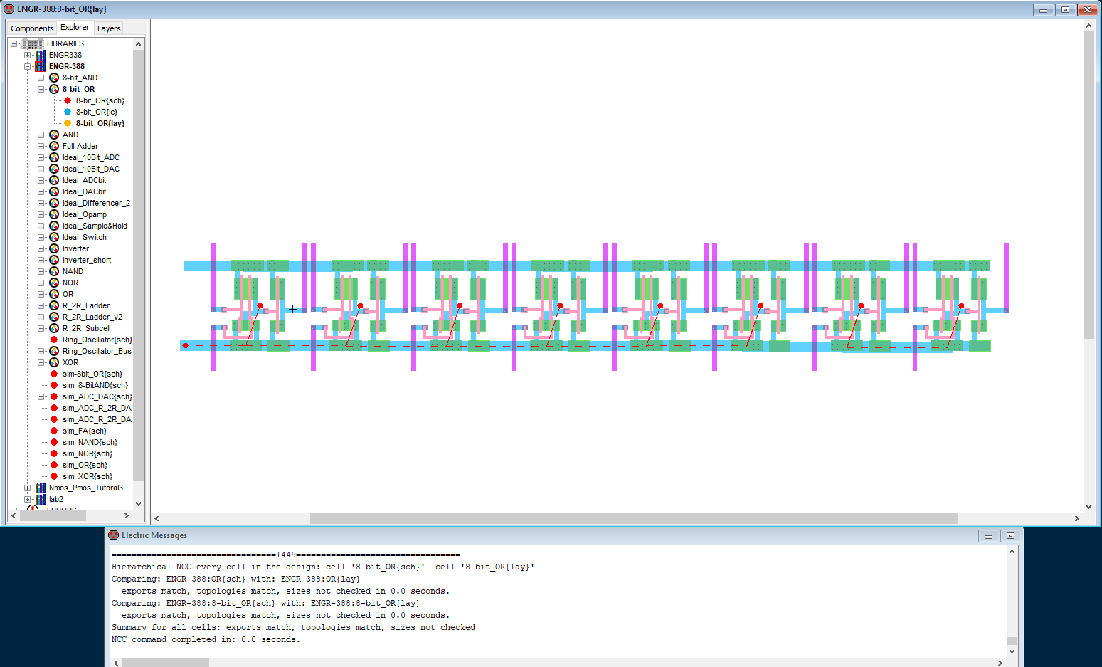
Figure 14: OR 8Bit Layout.


Task 4: 8-bit NAND gate
Task4_NAND-8Bit-Voltage.png
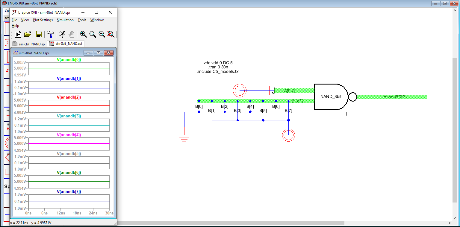
Figure 15: NAND 8-Bit Voltage.


Task4_NAND-8Bit-GND.png
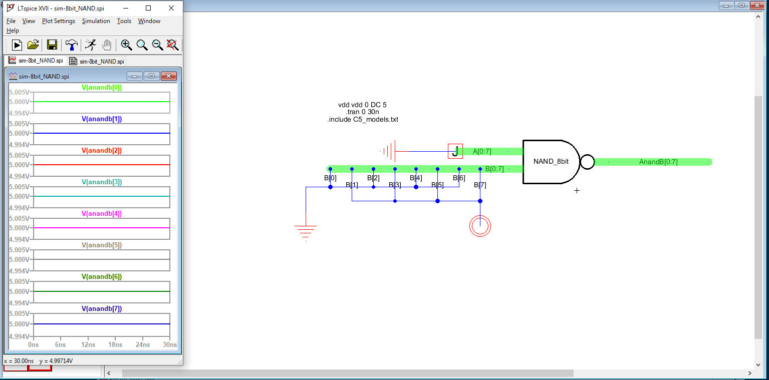
Figure 16: NAND 8-Bit GND.


Task4_NAND-8Bit-Layout.png
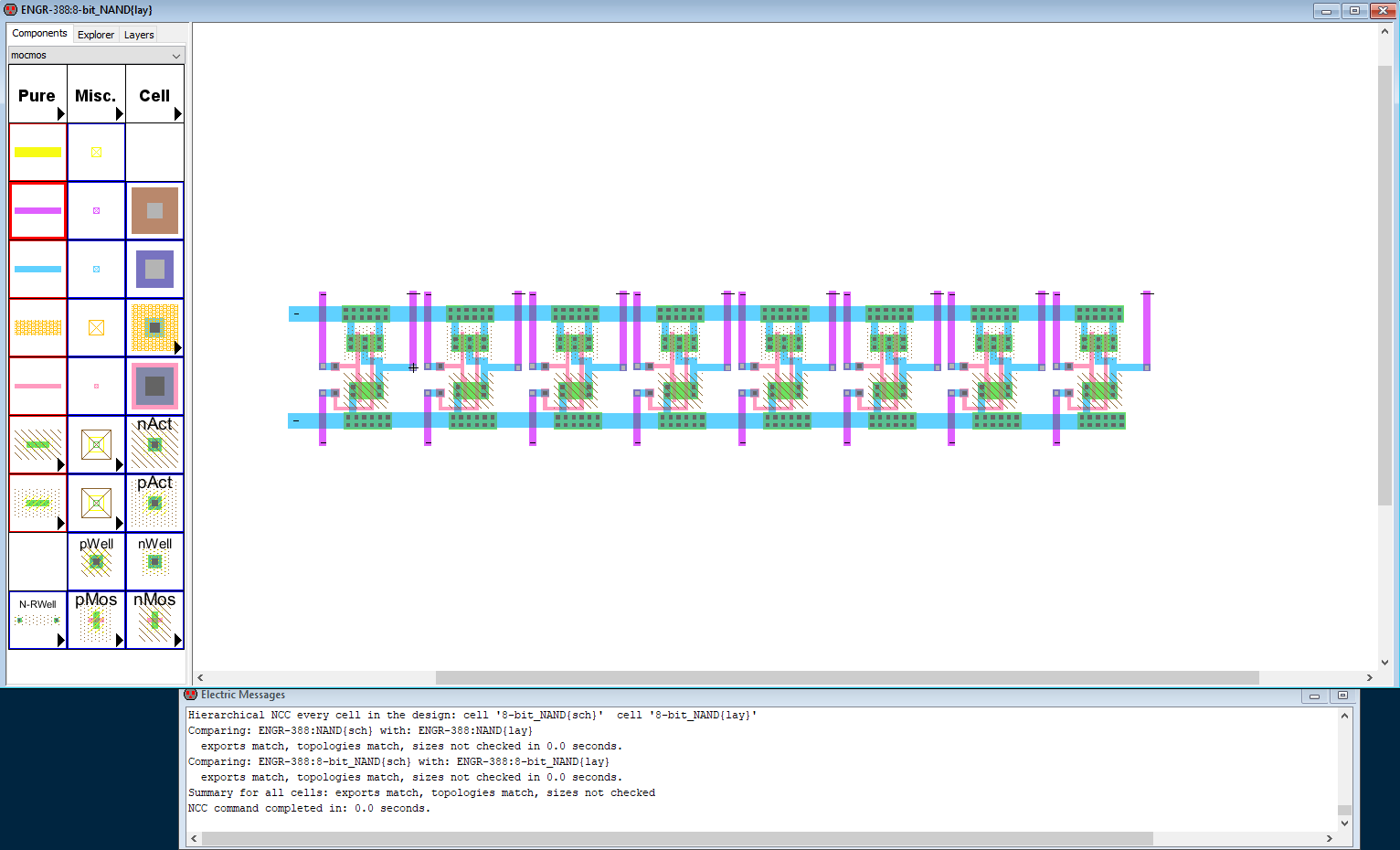
Figure 17: NAND 8-Bit Layout.


Task 5: 8-bit NOR gate
Task5_NOR-8Bit-Voltage.png
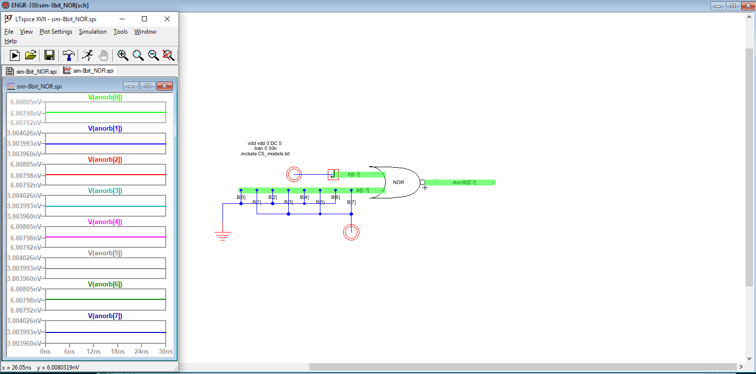
Figure 18: NOR 8-Bit Voltage.


Task5_NOR-8Bit-GND.png
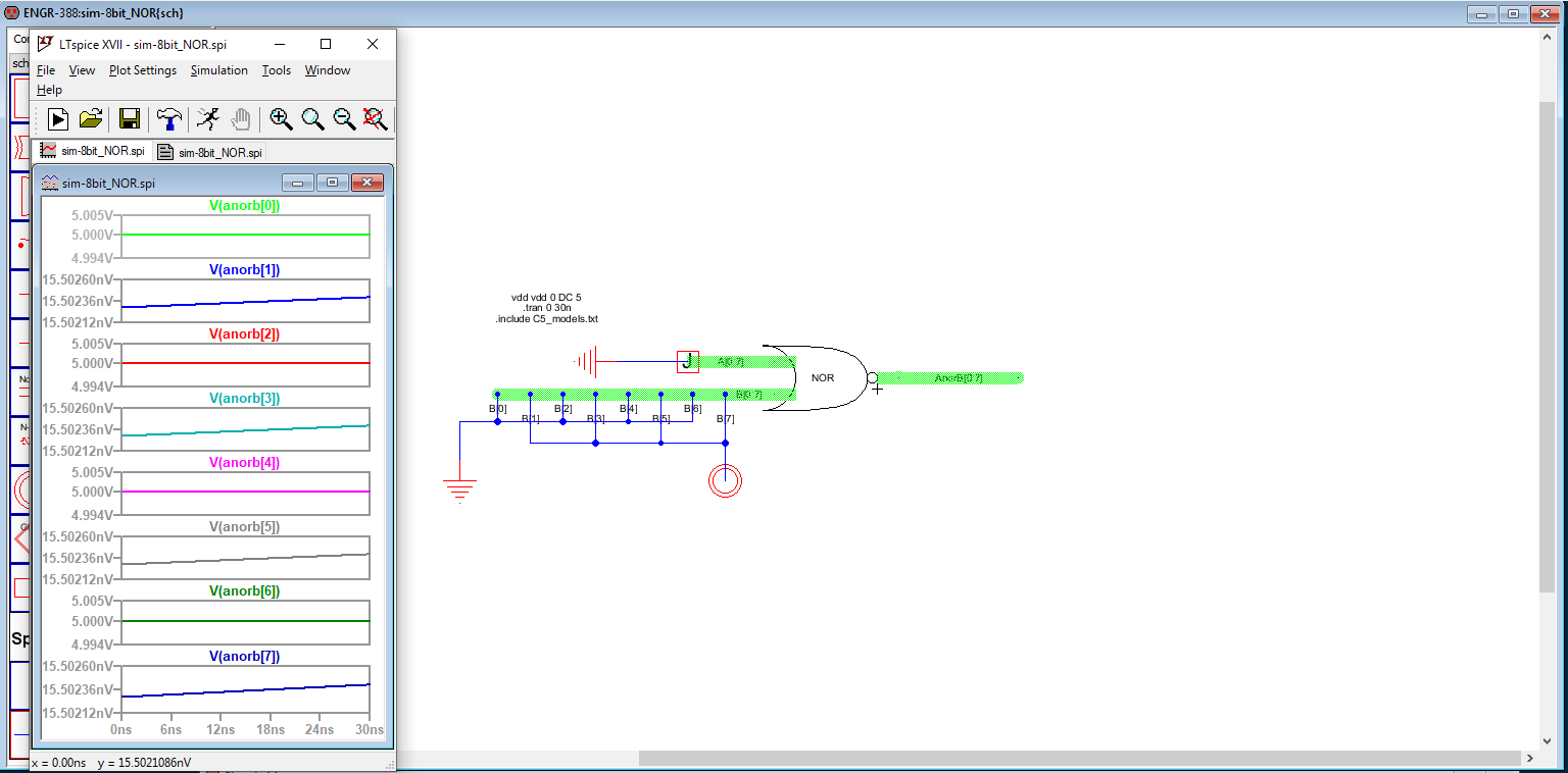
Figure 19: NOR 8-Bit GND.


Task5_NOR-8Bit-Schematic.pngTask5_NOR-8Bit-Schematic.pngTask5_NOR-8Bit-Schematic.png
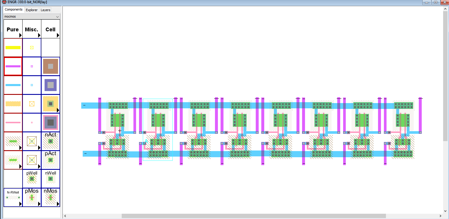
Figure 20: NOR 8-Bit Layout.


Discussion
Constructing the various 8-bit gates in Electric VLSI and simulating them gave an insight on how they are constructed and tested in the real world as well as the importance of  spacing for when you are constructin the 8-bit gates.