ENGR336 Lab 2022 Fall
Lab 6: NAND, NOR, XOR, and Full Adder
Name: Seth VanMatre
Email:
sgvanmatre@fortlewis.edu
NAND, NOR, XOR, and Full Adder
Introduction
The
objective of this lab is to layout and simulate a NAND, NOR, XOR, and Full Adder in Electric VLSI.
Materials and Methods
- Electric VLSI
Results
Task 1: Create the schematic and layout of the NAND gate.
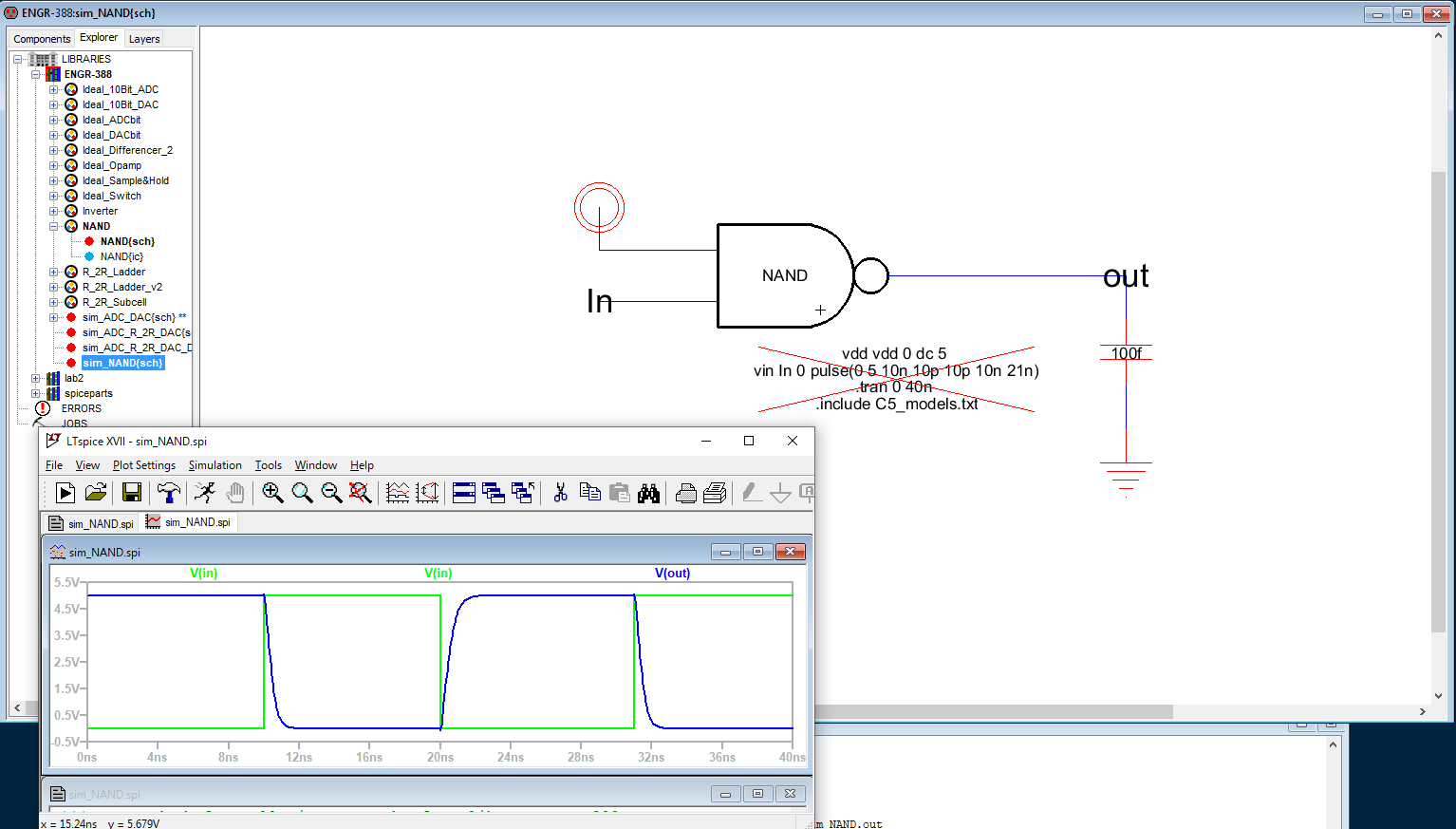
Figure 1: Simulated NAND gate.
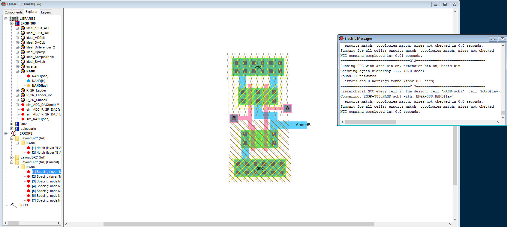
Figure 2: Created NAND layout.
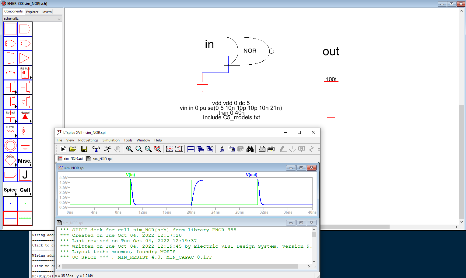
Task 2: Create the schematic and layout of the NOR gate.
Figure 3: Simulated NOR gate.
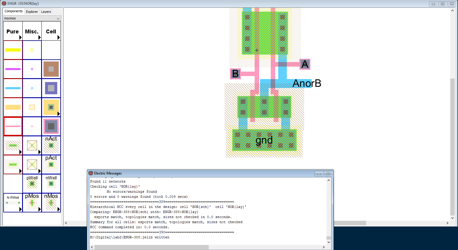
Figure 4: Created NOR layout.
Task 3: Design, simulte, and layout an XOR gate.
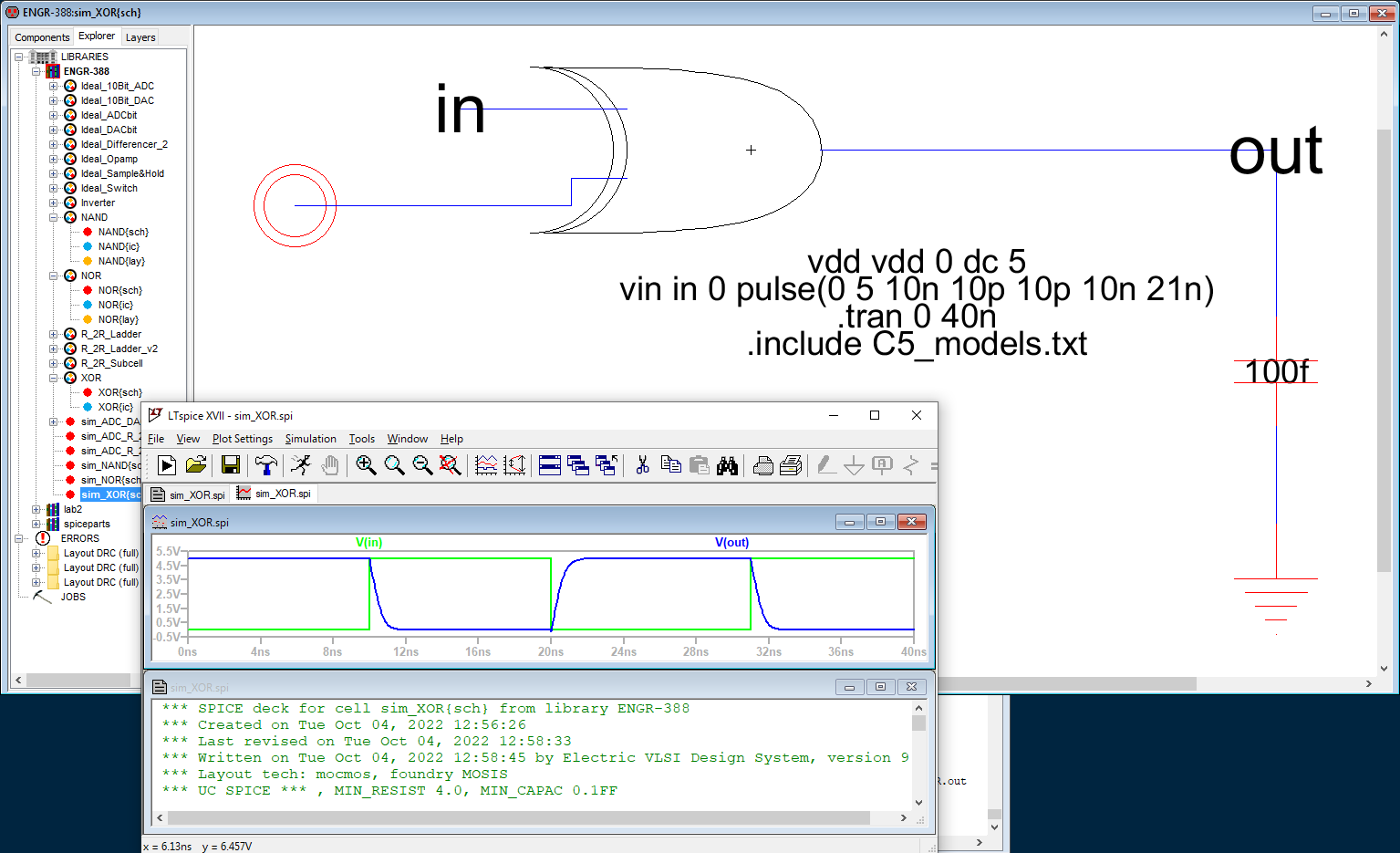
Figure 4: Simulated XOR gate.
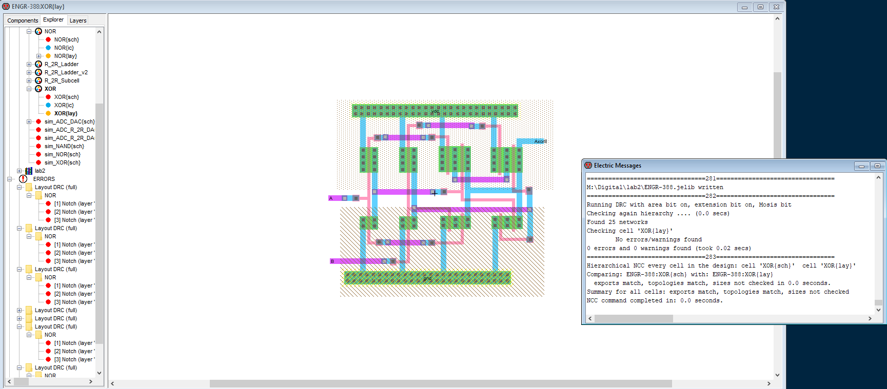
Figure 5: XOR layout.
Task 4: Design, simulate, and layout Full Adder
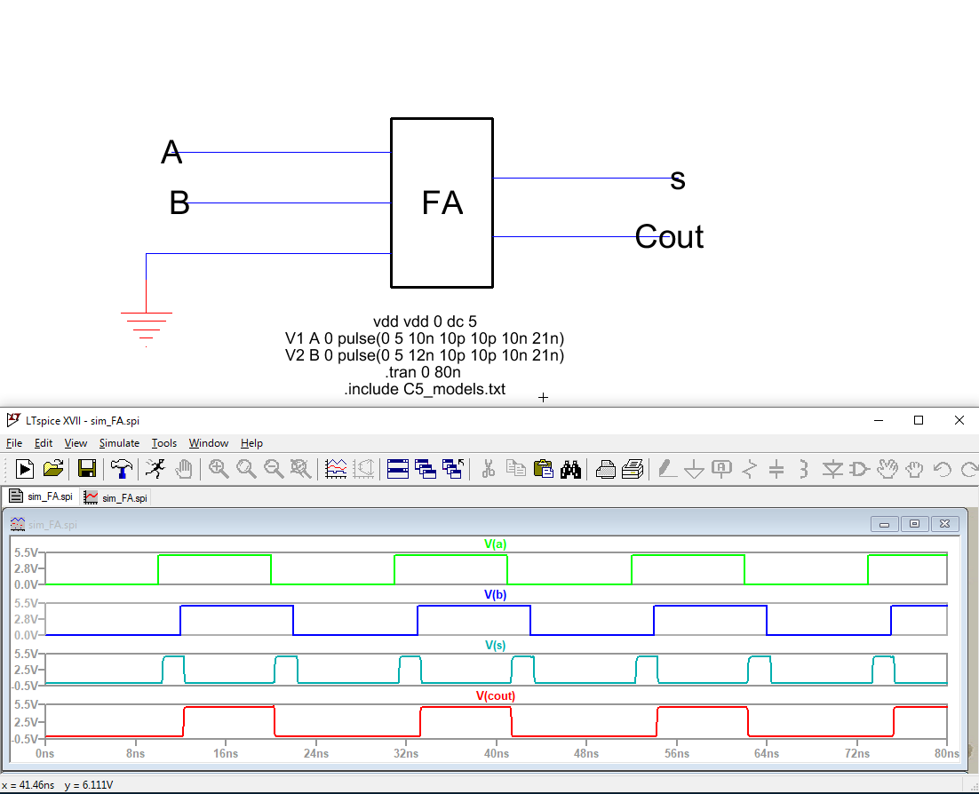
Figure 6: Simulated Full-Adder.
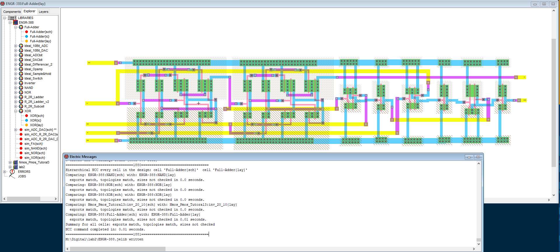
Figure 7: Full-Adder layout.
Constructing
the various gates in Electric VLSI and simulating them gave an insight on
how
they are constructed and tested in the real world as well as the
importance of matching up the input values so you don't get LRC errors.