ENGR336 Lab 2022 Fall
Lab 3: Layout the R-2R DAC
Name: Seth VanMatre
Email:
sgvanmatre@fortlewis.edu
Layout the R-2R DAC
Introduction
The
objective of this lab is to layout the R-2R DAC in Electric VLSI using
N-Well resistors as well as simulating the integrated circuit design in
LTSpice.
Materials and Methods
- Electric VLSI
- Download the libraries of the ideal ADC/DAC
Results
Task 1:
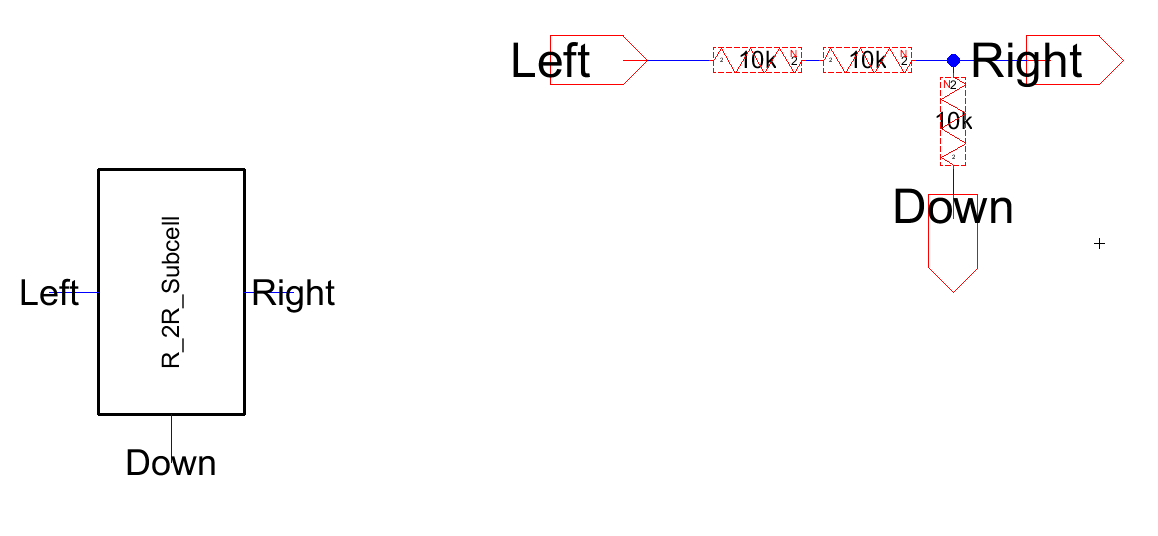
Figure 1: Circuit and schematic for R_2R_Subcell.
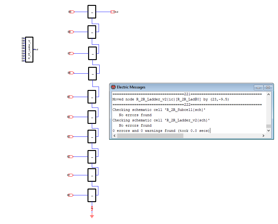
Figure 2: Built schematic of the subcells for the R-2R ladder.
Task 2:
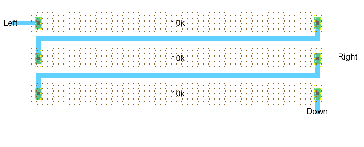
Figure 3: Built N-well resistors.
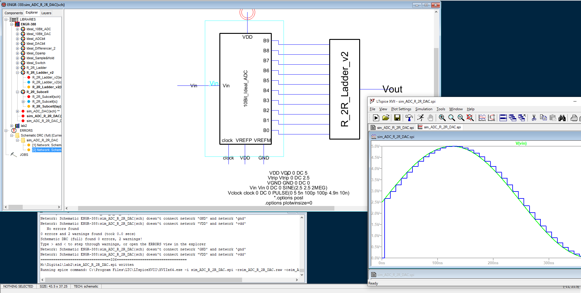
Figure
4: Constructed R_2R_Ladder using Figure 3 N-well resistors put into
configuration for 10-Bit DAC; Simulated using LTSpice.
Constructing
the R-2R DAC using N-well resistors was informative on how these
configurations are built and handled using Electric VLSI. It was also
intresting to build the N-well resistors and how their resistances are
a ratio of length/width.