ENGR336 Lab 2022 Fall
Lab 1: Review Superposition, Thevenin's Equivalent Circuit, and LTSpice
Name:
Seth VanMatre
Email: sgvanmatre@fortlewis.edu

Design an R-2R DAC

Introduction

The objective of this lab is to understand the operation of the ideal ADC and DAC as well as creating a R-2R DAC in Electric VLSI to replace the ideal DAC. The circuit will be simulated by using Electric VLSI  integrated with LTSpice.                                           

Materials and Methods

- Electric VLSI
- Download the libraries of the ideal ADC/DAC

Results

Task 1:
Ideal 10-bit DAC
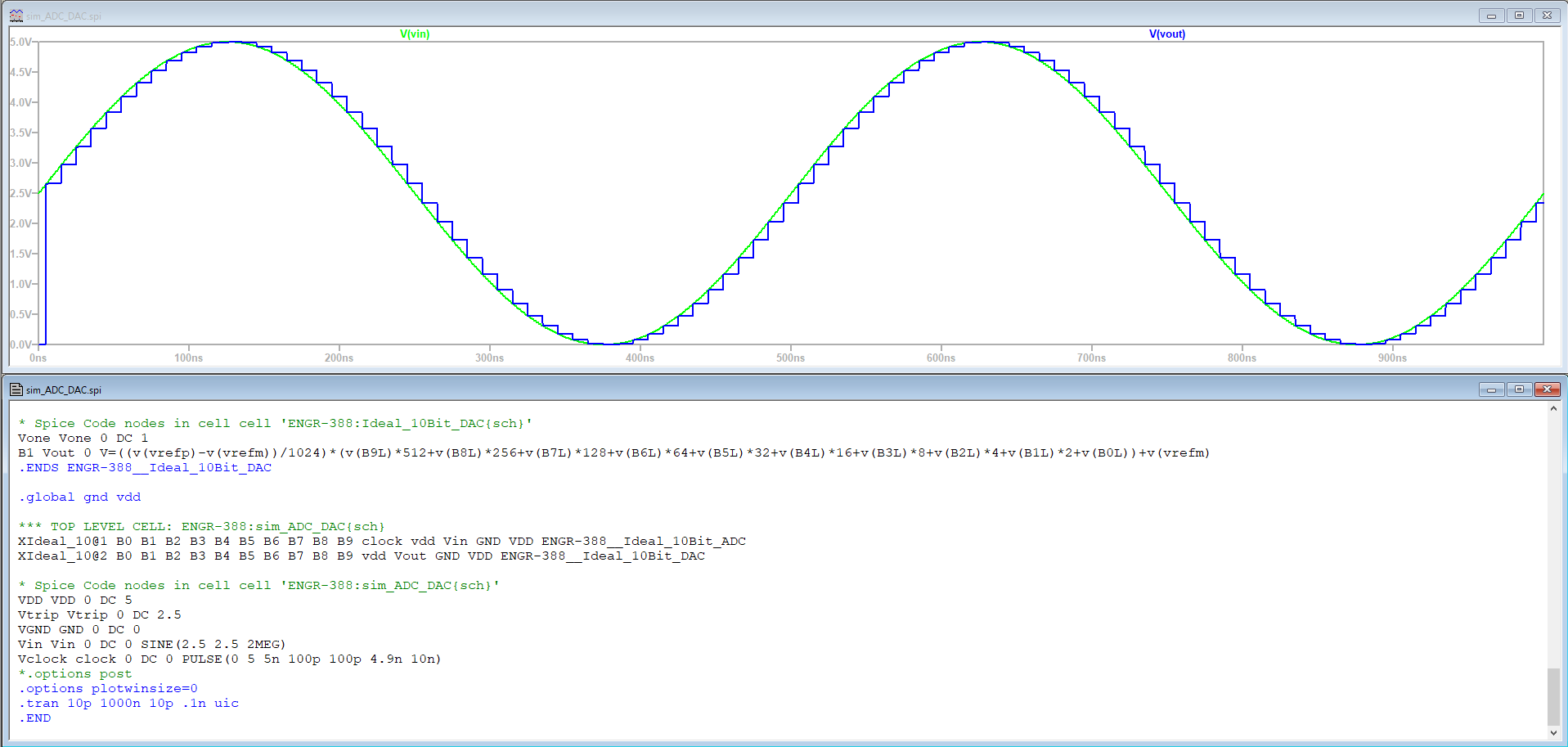
Figure 1: Ideal output for a 10-bit DAC; Simulated using Electric VLSI and LTSpice integrated circuit design.
Task 2:
Built 10-bit DAC simulated
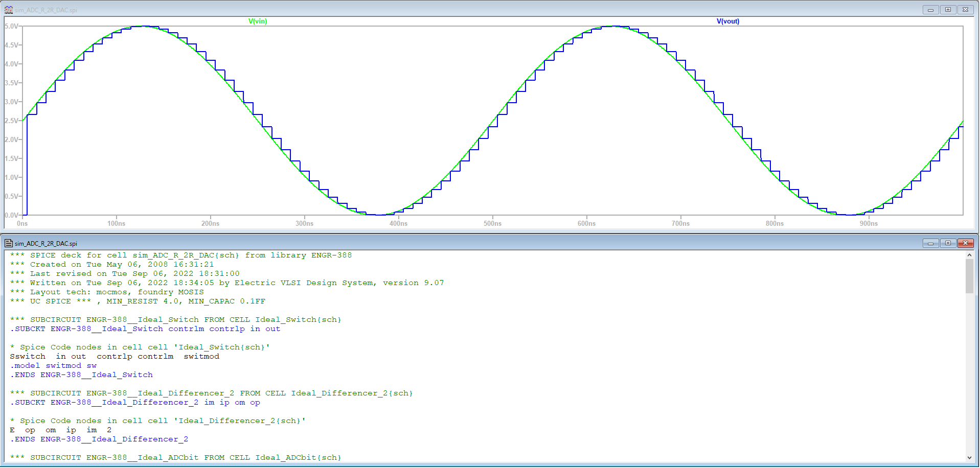
Figure 2: Constructed R-2R DAC ouput; Simulated using Electric VLSI and LTSpice integrated circuit design.
Task 3:
Time Delay Load
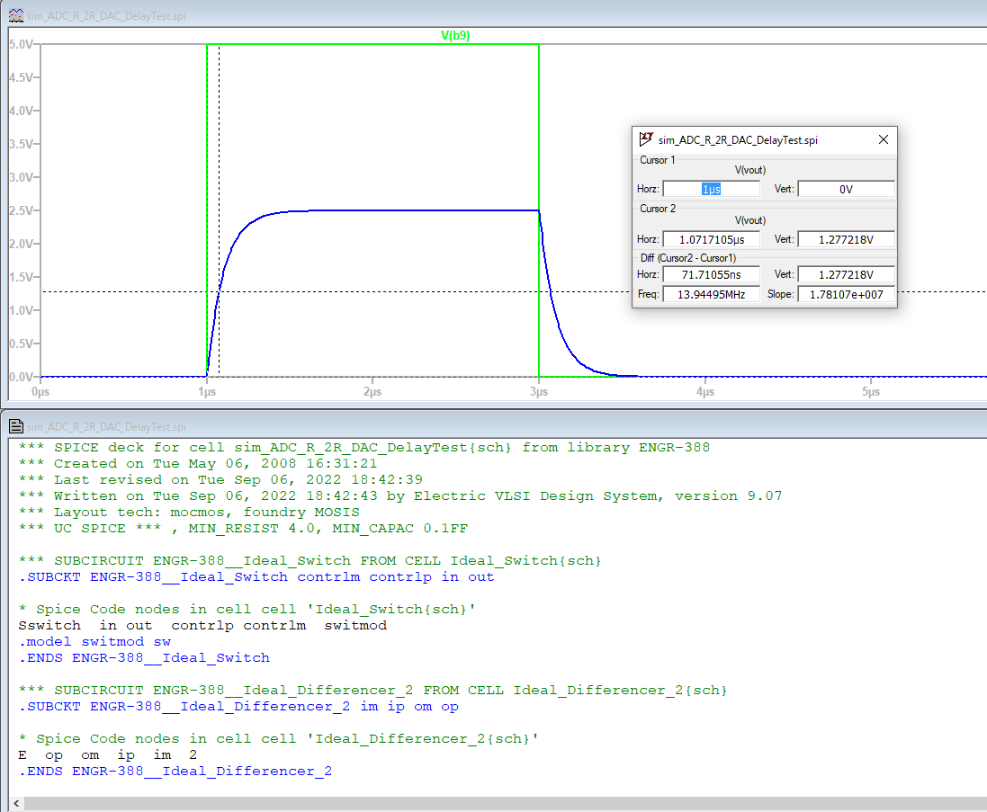
Figure 3: Time delay from B9 pin when the DAC drives a 10pF load; Simulated using Electric VLSI and LTSpice integrated circuit design.


Hand Calc
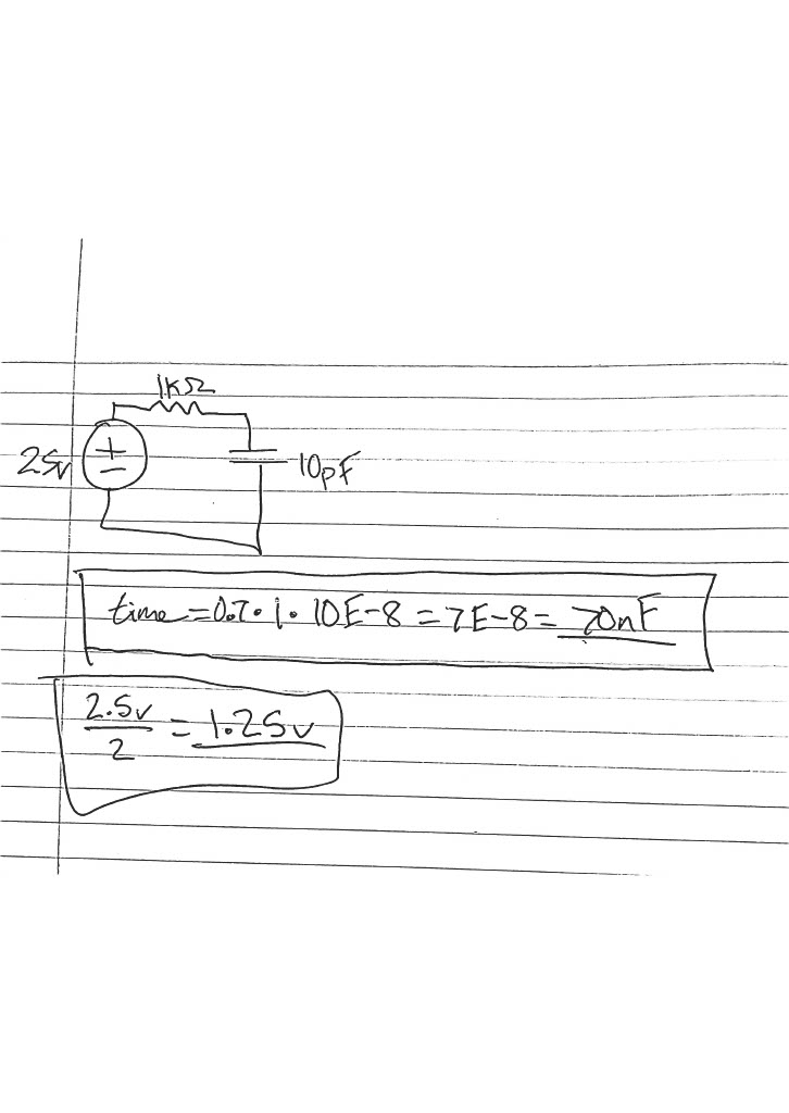
Figure 4:  Hand calculations for the how long it takes the capacitor to charge half way; Thevenin's Cirucit.

The calculation for how long it would take the capacitor to charge half way matched with the simulation resutls.
Discussion
Creating a R-2R DAC was fun, especially seeing it work on a load and output what was calcuated. Unfortunately, I wasn't able to get back into the embeded lab where the Electric VLSI was downloaded so I wasn't able to capture images of the schematic of my R-2R DAC as well as having only pin B9 driving the load.