ENGR336 HW8 2022 Fall
HW8: Cadance Tutorials 1-2

Name: Seth VanMatre
Email: sgvanmatre@fortlewis.edu

Cadance Tutorials 1 and 2

Introduction

The objective of this lab is to learn how to operate cadance as well as finish the tutorial 1 and 2.      

Materials and Methods

- Cadance

Results

Tutorial 1: V-divider
v-divider
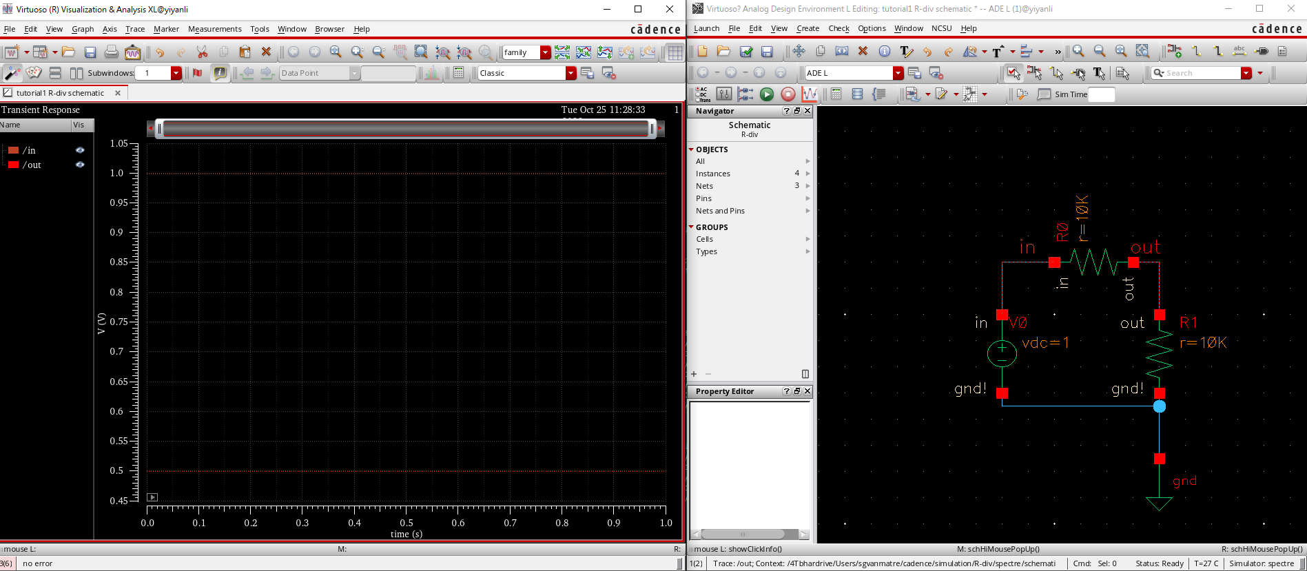
Figure 1: Simulated v-divider using 10k ohm resistor.


Symbol V-divider
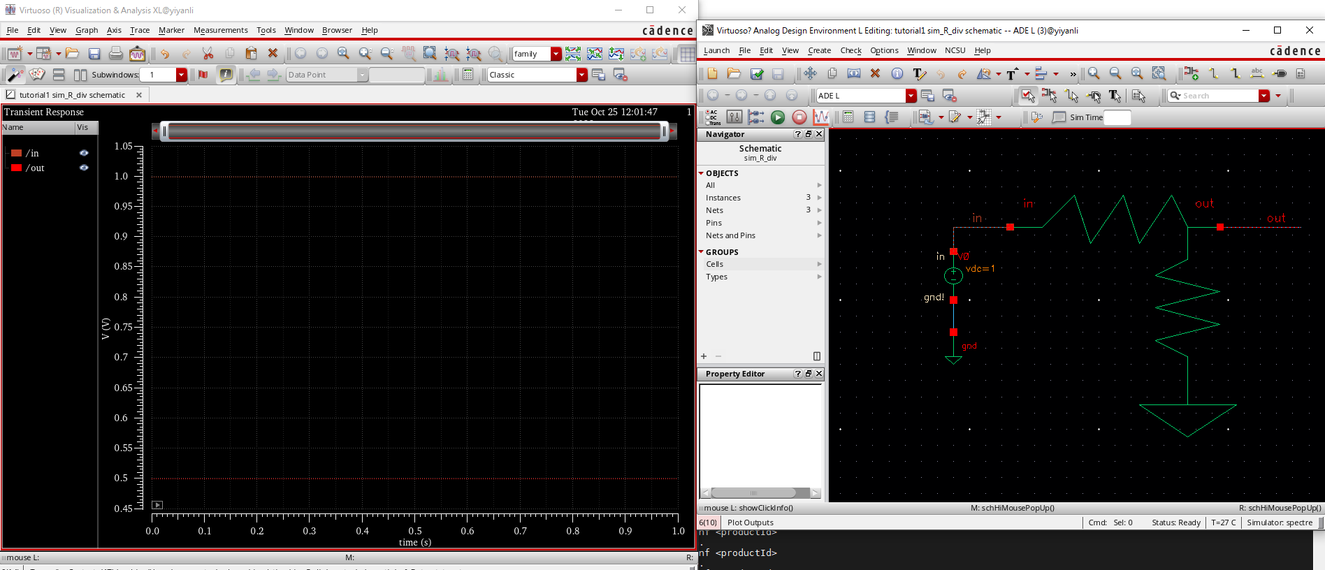
Figure 2: Simulated symbol for Figure 1.


Nwell10k
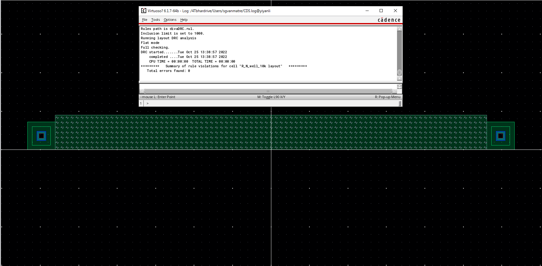
Figure 3: Nwell 10k ohm.

Layout
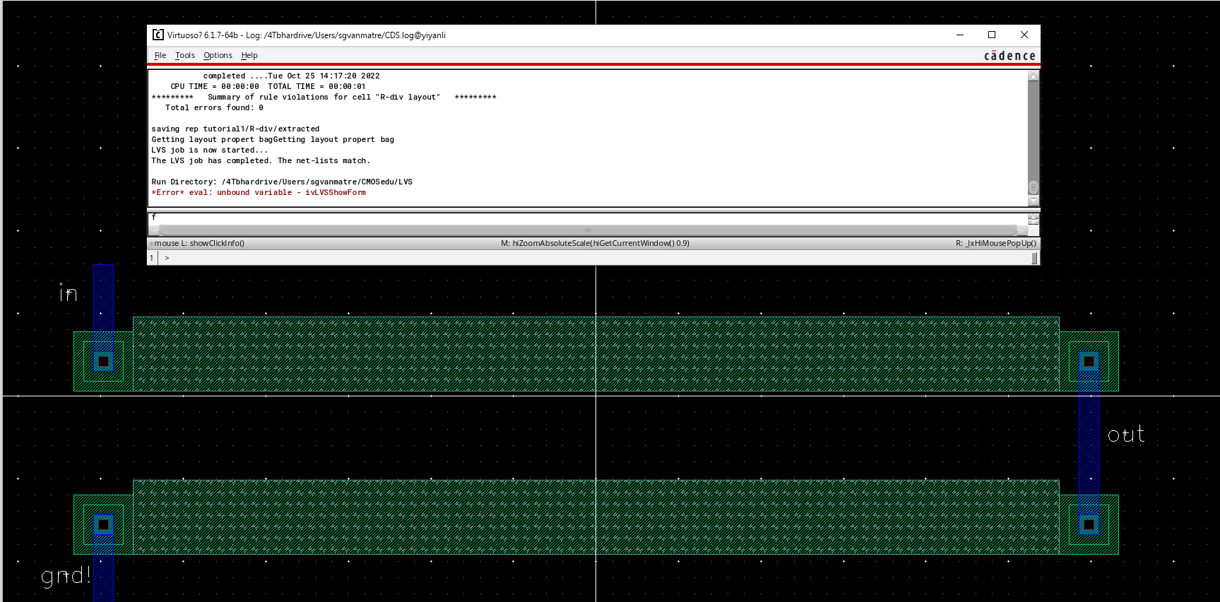
Figure 4: V-divider layout passing LRC.


Tutorial 2: NMOS and PMOS
NMOS
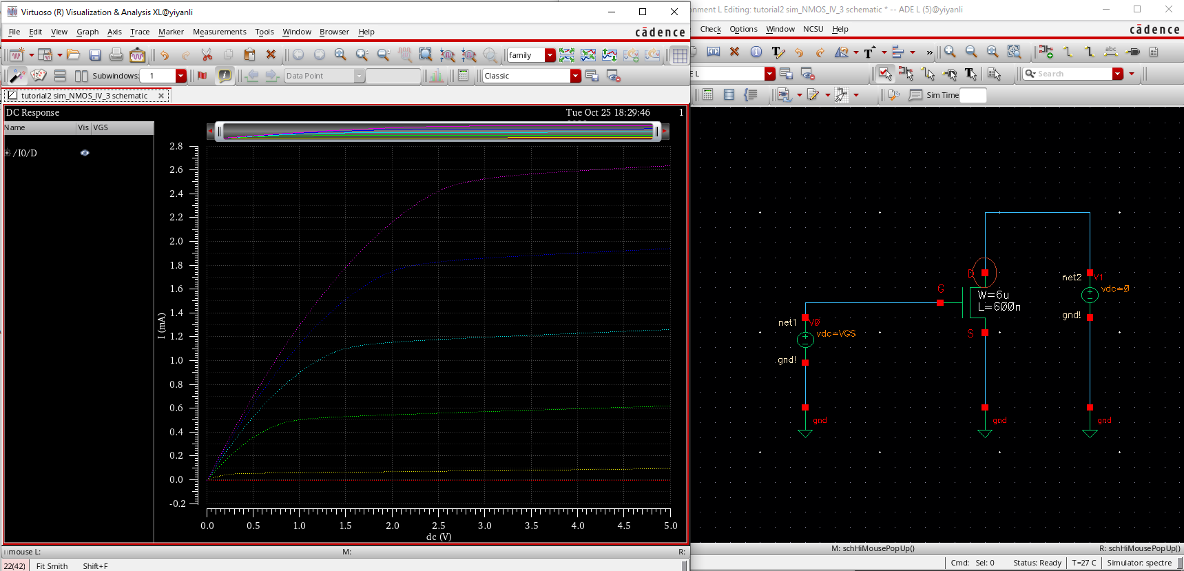
Figure 5: Simulated NMOS.

NMOS ERROR
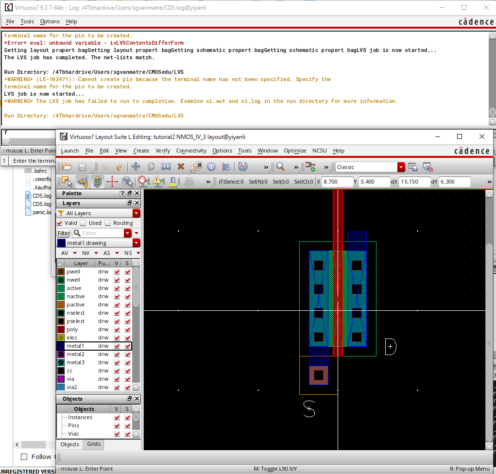
Figure 6: NMOS encountered error layout.

4thPin
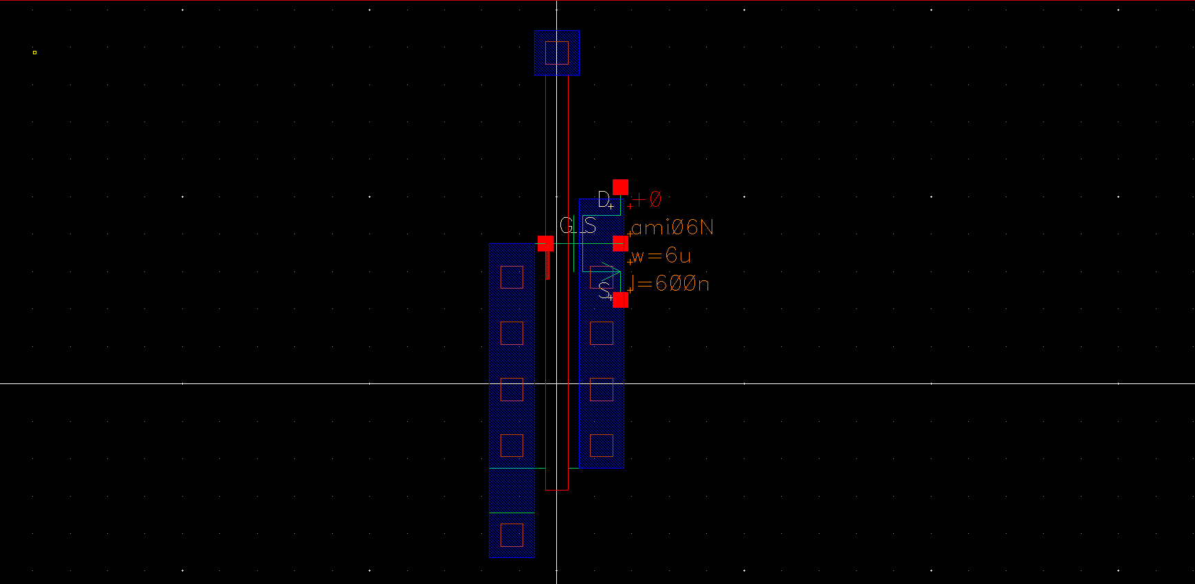
Figure 7: NMOS body pin.

Extracted Sim
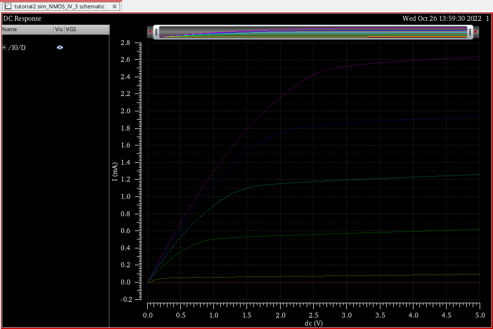
Figure 8: Extracted NMOS.


PMOS schematic
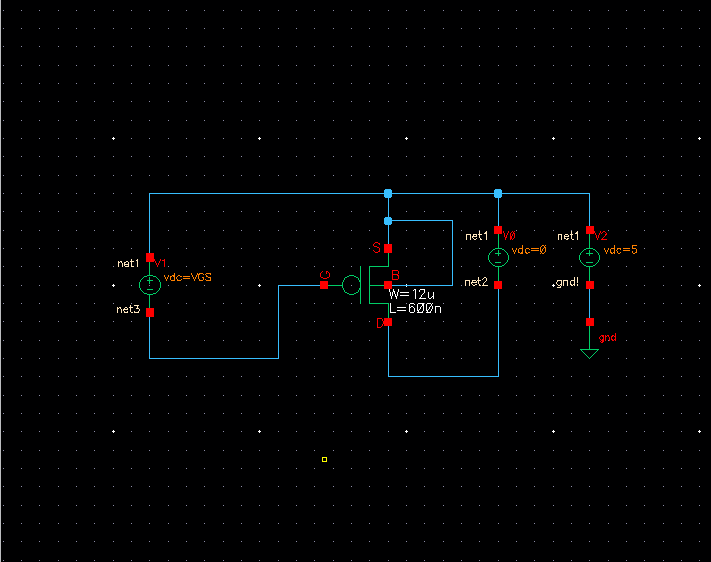
Figure 9: PMOS schematic.

PMOS simulated schematic
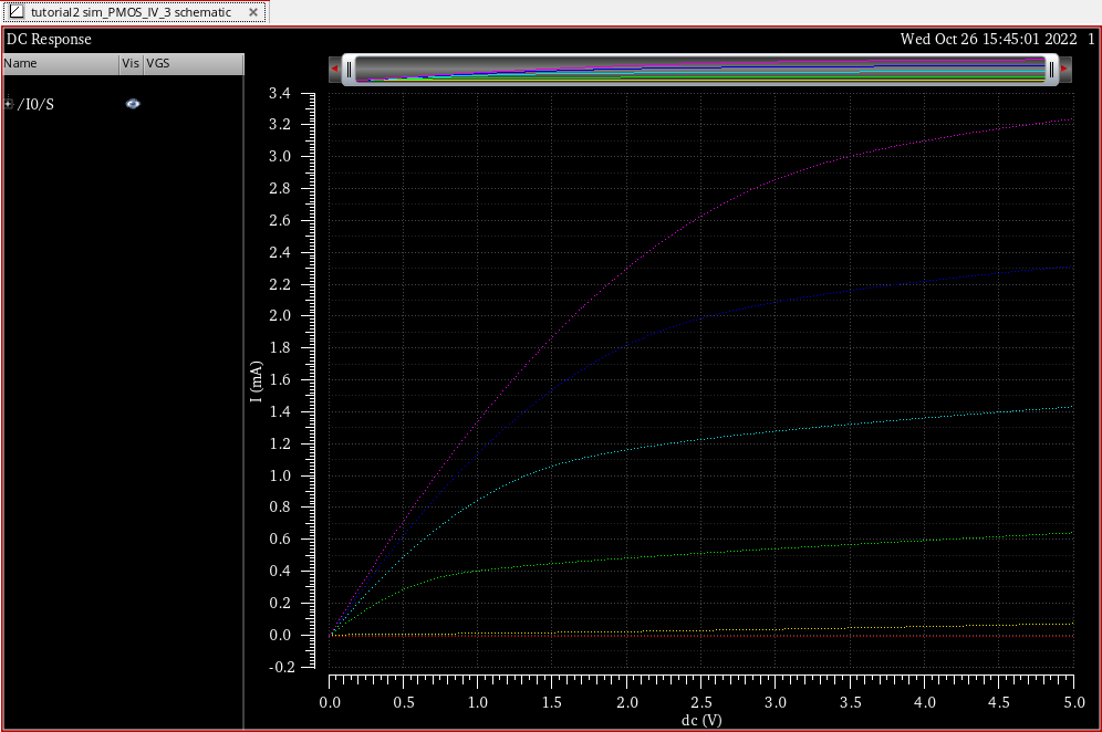
Figure 10: Simulated PMOS schematic.

PMOS layout
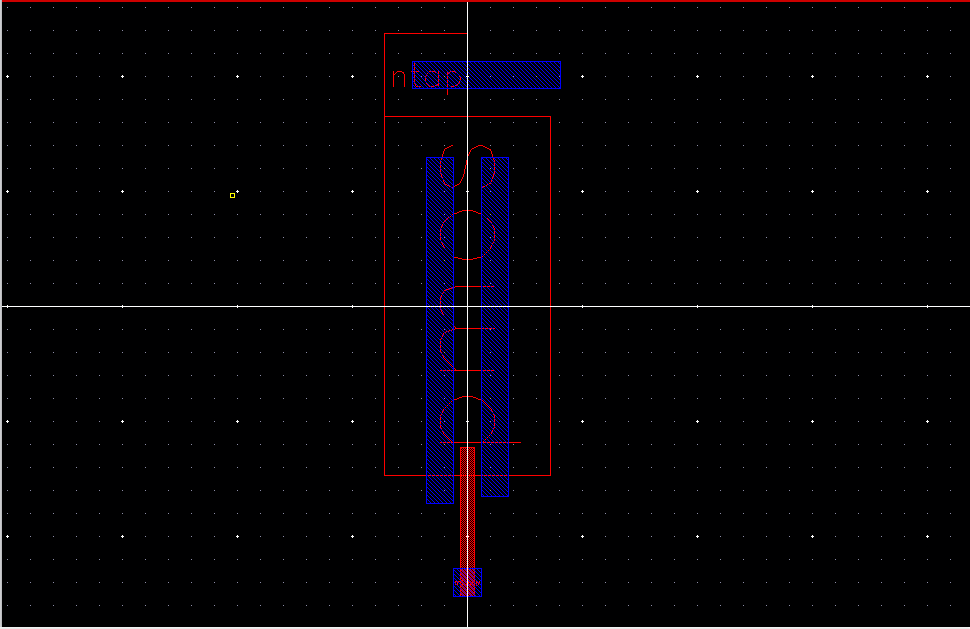
Figure 11: PMOS layout.

PMOS extracted
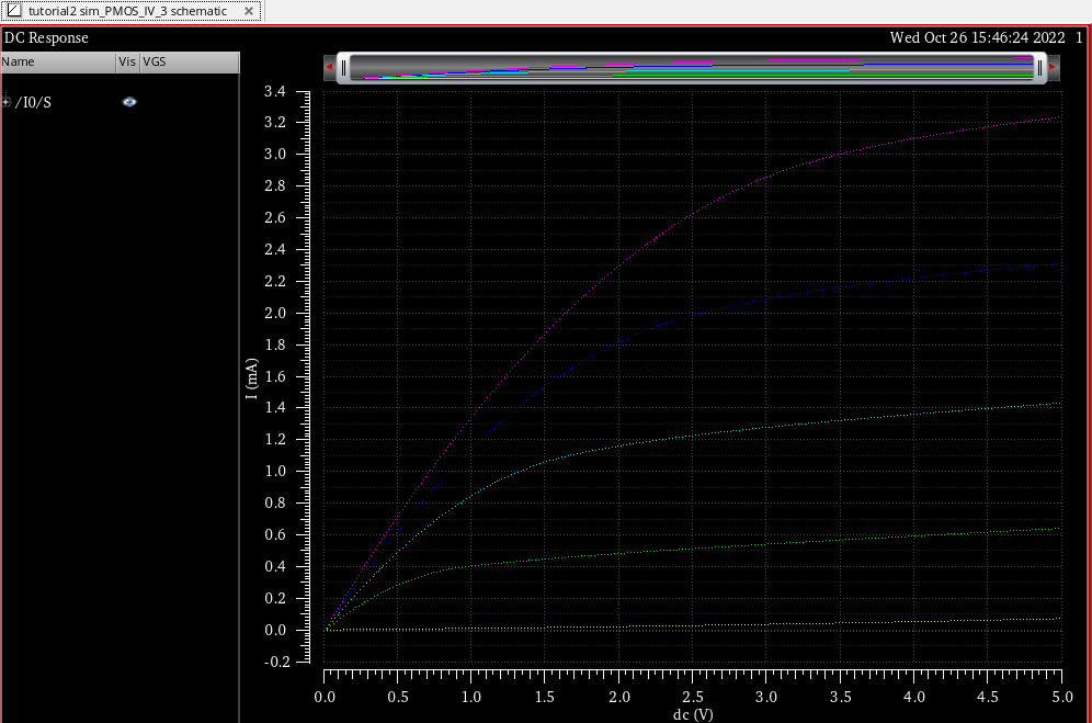
Figure 12: PMOS extracted layout simulated.


Discussion
Using Cadance helps me understand how IC designs are used in the real world as well as how they are deveopled using this program.