ENGR 433 Lab 2023 Spring
Lab 3: Seven-Segment Display on An FPGA
Name:
Seth VanMatre
Email: sgvanmatre@fortlewis.edu

Introduction to FPGA

Introduction

The objective of this lab is to demonstrate combinational logic blocks on both simulation and board as well as using the seven-segment display.

Materials and Methods
- Install Vivado 2018 version.


Results
Task 1: Simulate and implement the following combinational logic blocks:
       - Inverter
       - 2-bit full adder
       - 8-bit And
       - 4-1 MUX

inverterCode.png
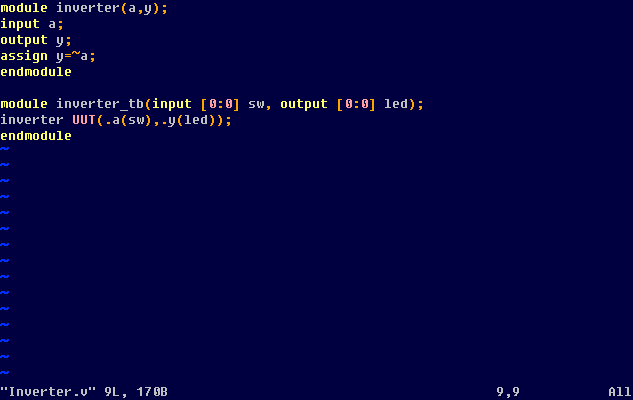
Figure 1: Inverter code.

inverterSim.png
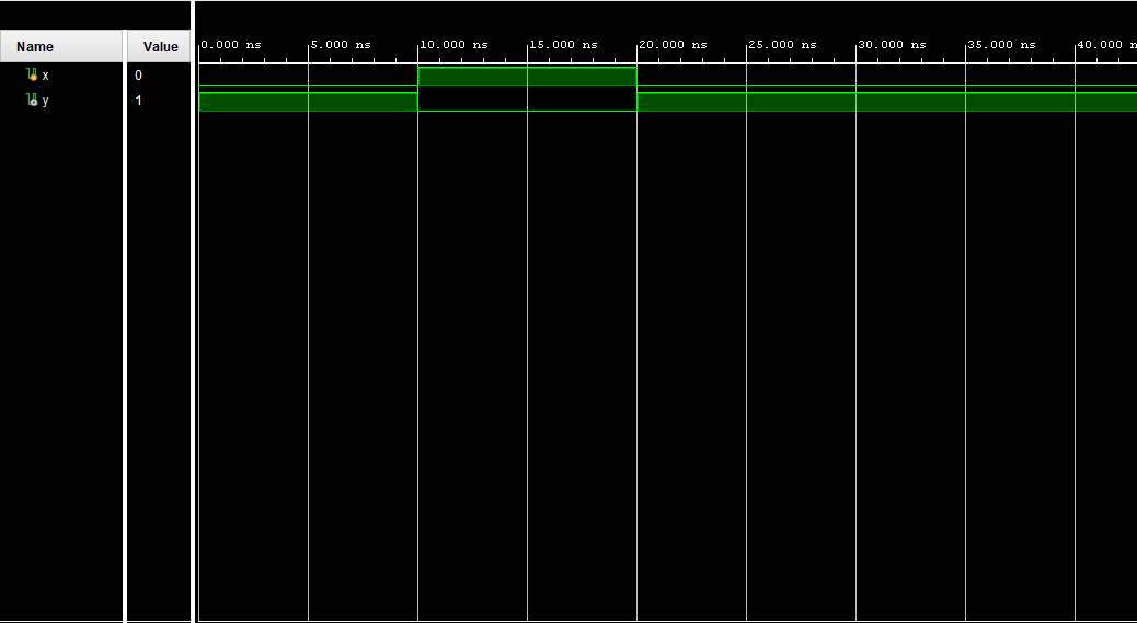
Figure 1.1: Inverter simulation.

InverterBoardOFF.jpg
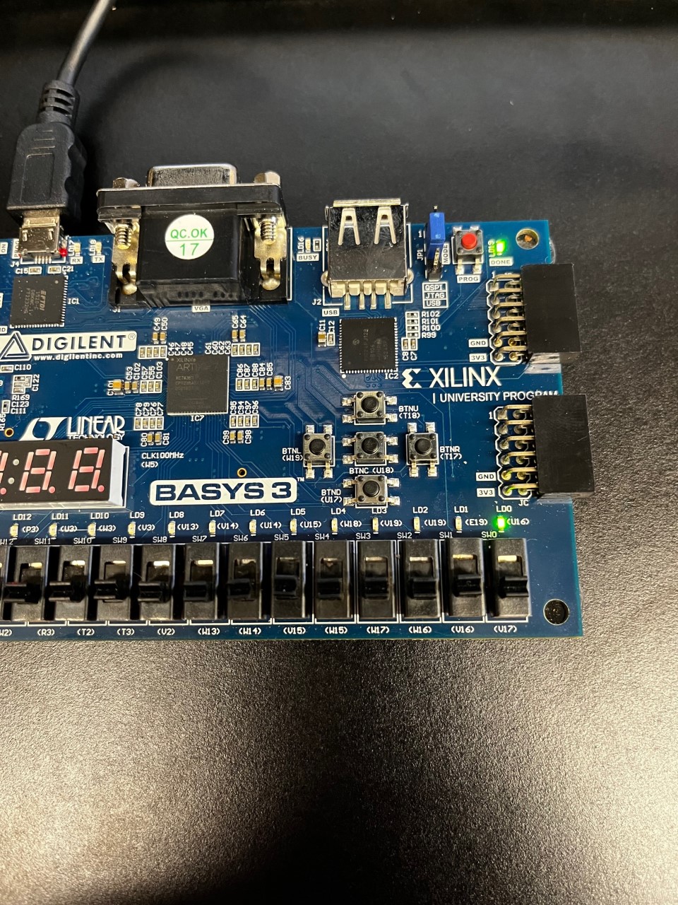
Figure 1.2: Inverter implemented ON output.

InverterBoardON.jpg
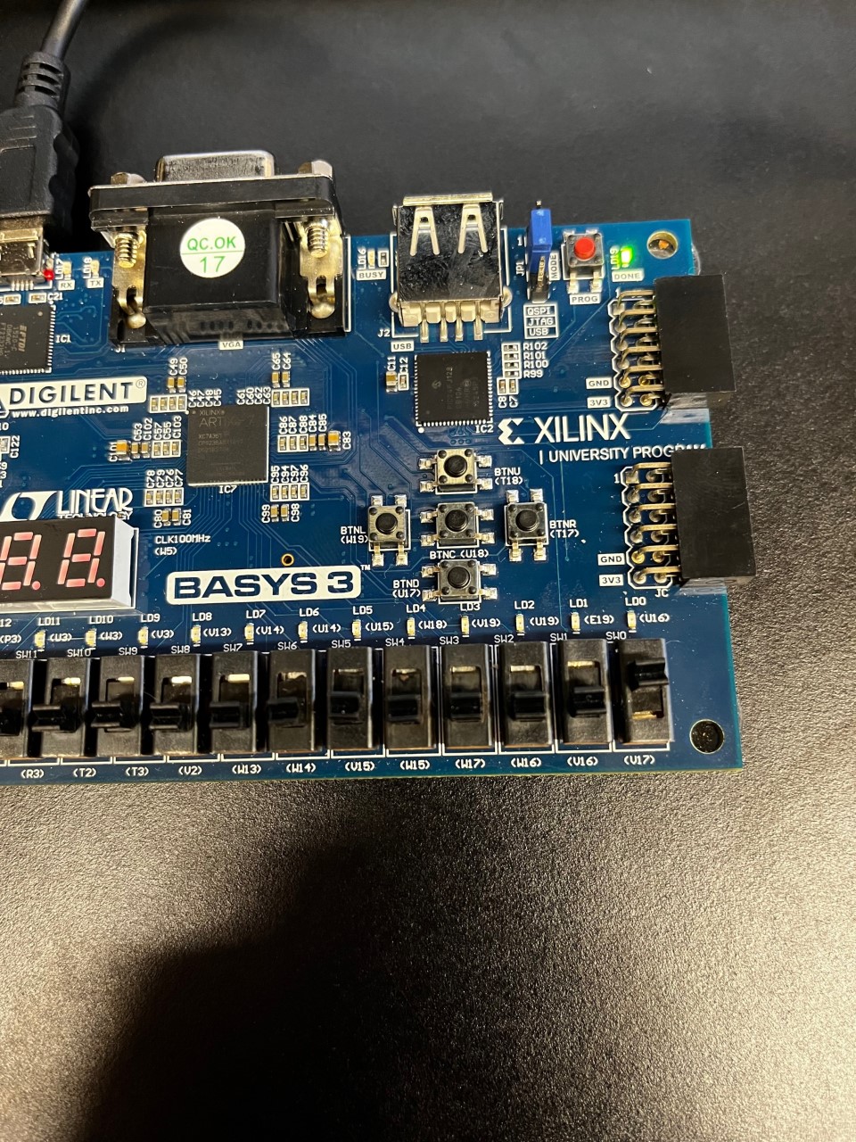
Figure 1.3: Inverter implemented OFF output

TwoBitFullAdderCode.png
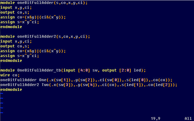
Figure 1.4: 2-bit full adder code.

TwoBitFullAdder.png
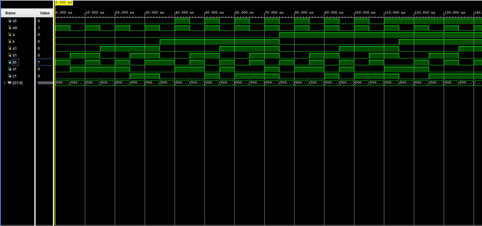
Figure 1.5: 2-bit full adder simulation.


EightInputANDCODE.png
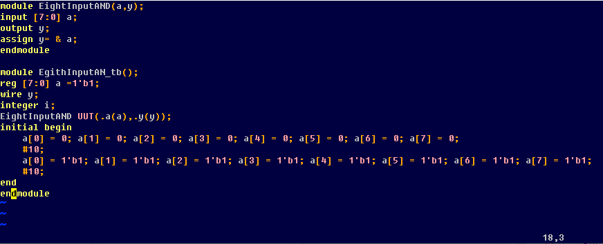
Figure 1.6: 8-bit AND code.

MUX4x1Sim.png
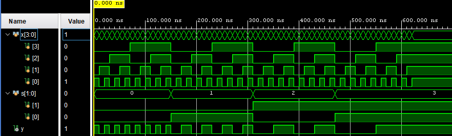
Figure 1.7: 8-bit AND simulation.


MUX4x1Code.png
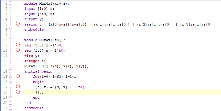
Figure 1.8: 4-1 MUX code.

MUX4x1Sim.png
Figure 1.9: 4-1 MUX simulation.


Task 2: Using Verilog and Viado to design a 'Running LED' program on the FPGA board.

SSDisplayCode.pngRunningLed.png
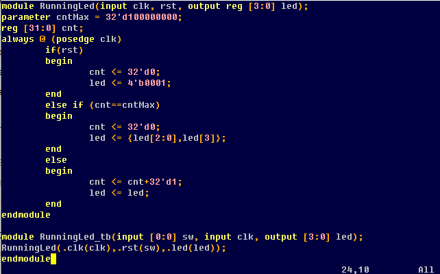
Figure 2: Running LED code.


Task 3: Interface the switches with the 7-segment display on the board.

SSDisplayCode.png
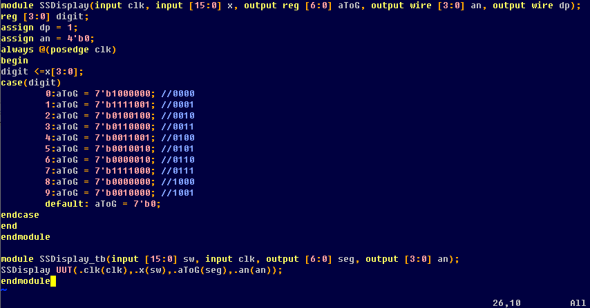
Figure 3: SSDisplay code for all sections.


SSDisBoard.png
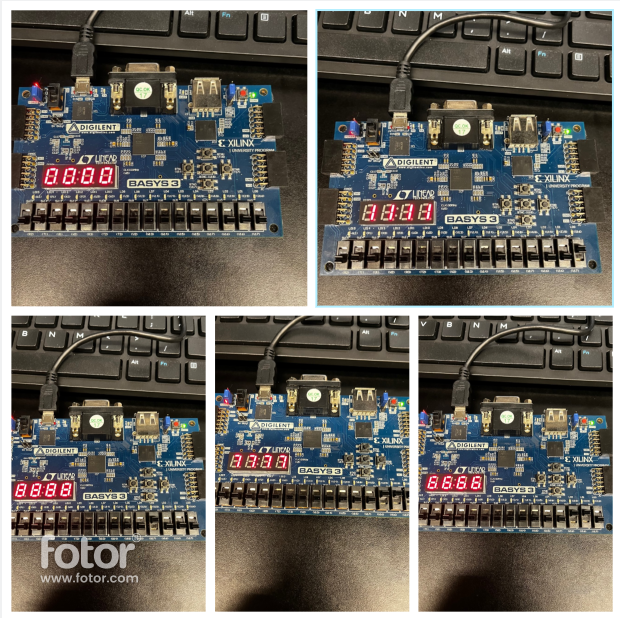
Figure 3.1: Implementation of SSDisplay to board.

Task 4: Modify the code in  task 3 to only show the number on one of the displays.

LCDCode.png
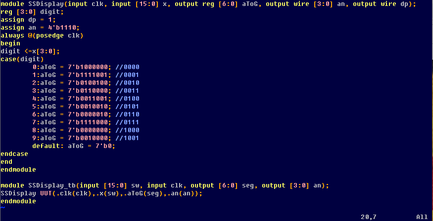
Figure 4: SSDisplay for only having one of the displays on.


Discussion
HDL utilizes the activation of  programmable field arrays making the structure of HDL different to any programming language. New approaches can be taken on a problem by using the clock of the FPGA board or just by using simple logic.