Task 1: Logic equations.
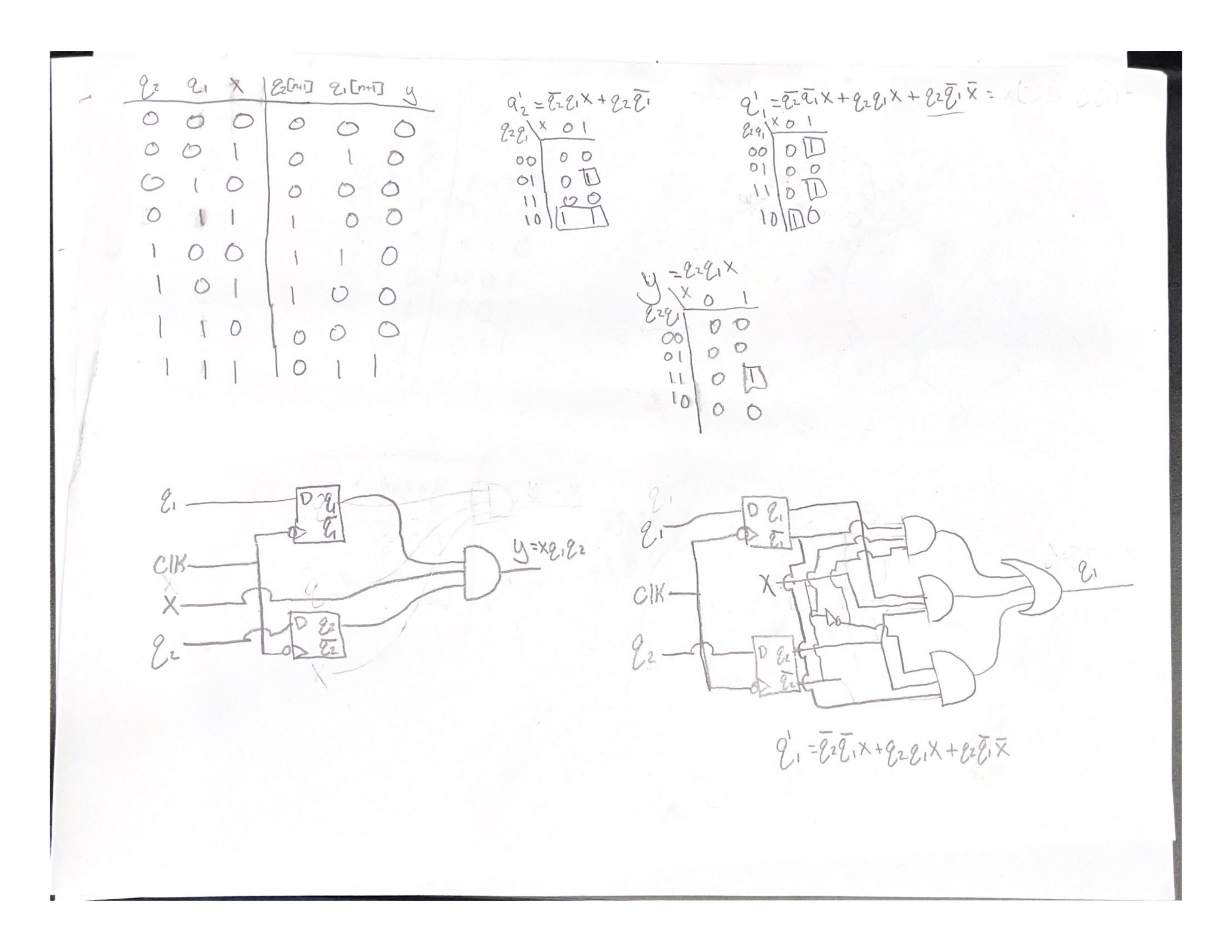
Figure 1: Logic equations and seqential circuit.
Task
2: Behavioral and logic simulation results.
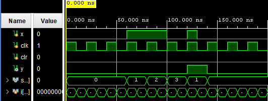
Figure 2: Logic block simulation results.
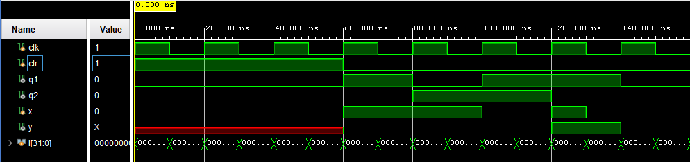
Figure 2.1 Behavioral simulation results.
Task 3: Sequence Detector 1011.
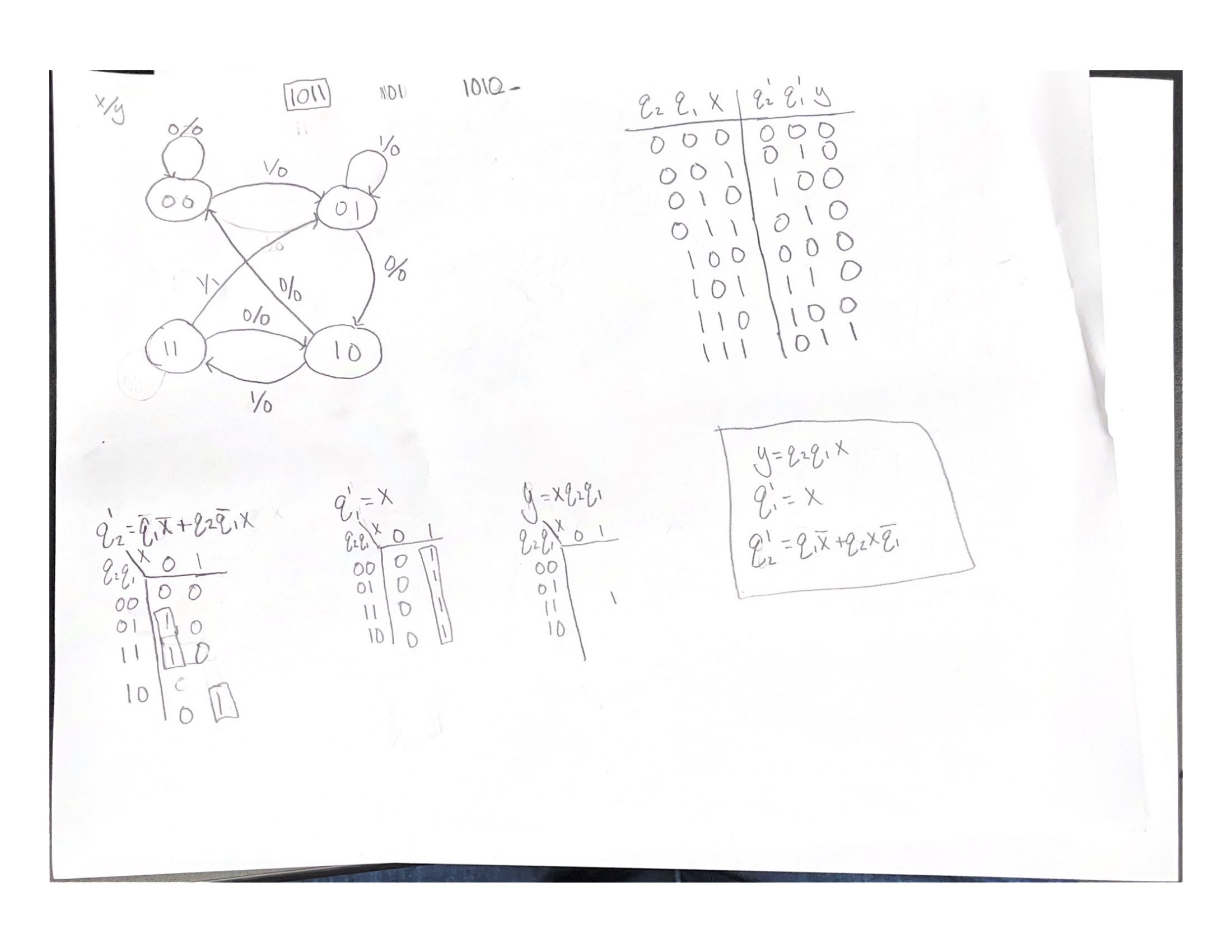
Figure 3: State diagram for the sequence detector 1011.
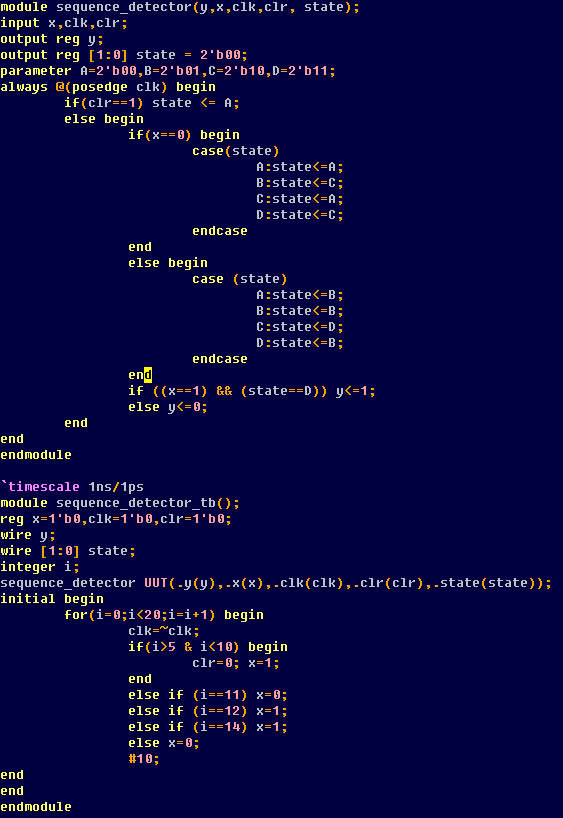
Figure 3.1: Code for sequence detector 1011.
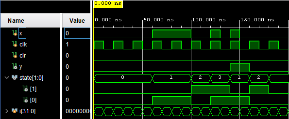
Figure 3.2: Simulation for sequence detector 1011.
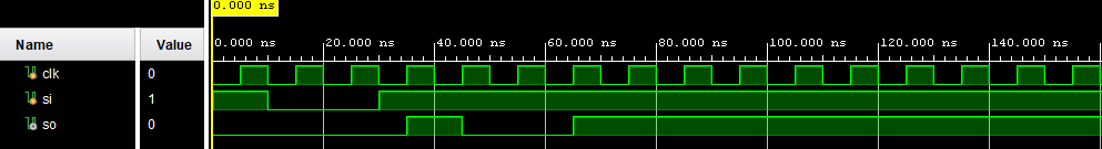
Figure 4: SISO simulation.
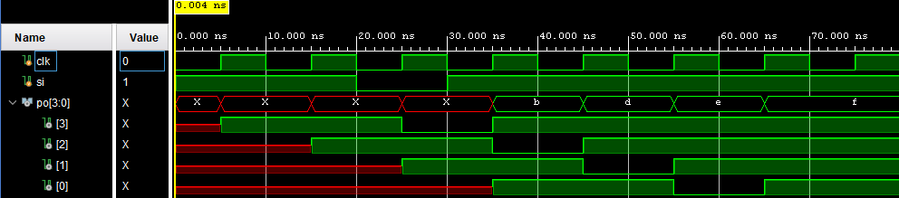
Figure 4.1: SIPO simulation.
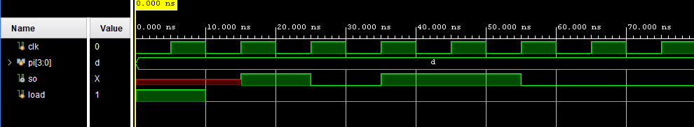
Figure 4.3: PISO simulation.
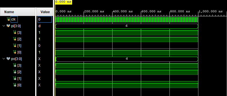
Figure 4.4: PIPO simulation.
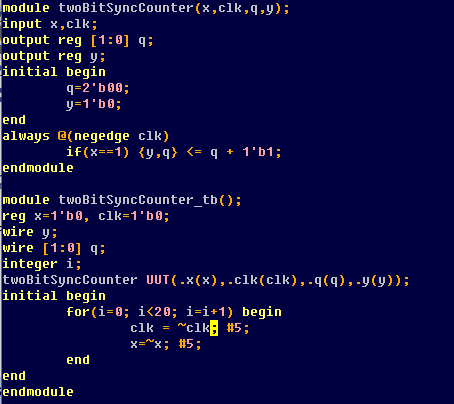
Figure 5: Two bit counter code.
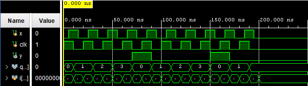
Figure 5.1: Two bit counter simulation.
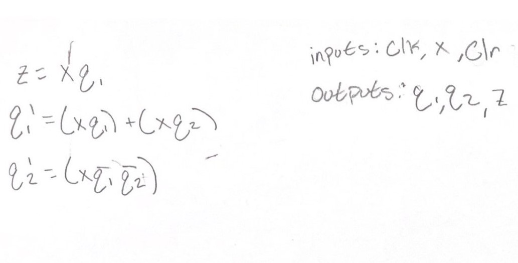
Figure 6: Logic equations of the circuit.
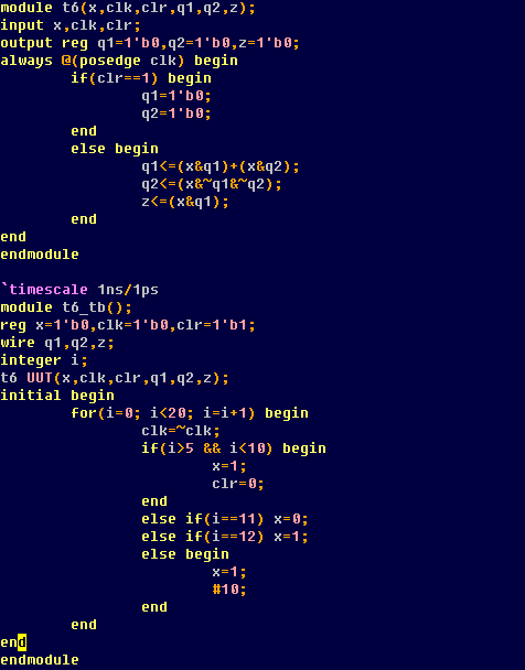
Figure 6.1: Code for the logic.
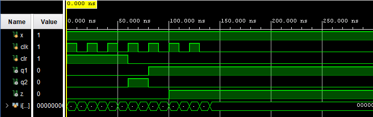
Figure 6.2: Simulation of the logic.
Figure 2: Logic block simulation results.
Figure 2.1 Behavioral simulation results.
Task 3: Sequence Detector 1011.
Figure 3: State diagram for the sequence detector 1011.
Figure 3.1: Code for sequence detector 1011.
Figure 3.2: Simulation for sequence detector 1011.
Task 4: Simulation for the four types of shift registers.
Figure 4: SISO simulation.
Figure 4.1: SIPO simulation.
Figure 4.3: PISO simulation.
Figure 4.4: PIPO simulation.
Task 5: Counter module and simulation.
Figure 5: Two bit counter code.
Figure 5.1: Two bit counter simulation.
Task 6: Logic equation for the circuit as well as implmentation and simulation.
Figure 6: Logic equations of the circuit.
Figure 6.1: Code for the logic.
Figure 6.2: Simulation of the logic.