CE 433 Spring 2024 Lab 3: More about FPGA- Seven Segment Display Sahra Genc sggenc@fortlewis.edu
LAB 3:More about FPGA - Seven Segment Display
Introduction: In this lab assignment, we were tasked to
construct an inverter, a 2-bit full adder, an 8-input AND gate, and a
4-to-1 multiplexer. We conducted simulations and used on-board
verification to validate the logic. Additionally, we were assigned the
task of design a program for running LEDs on the FPGA board, first with
four LEDs, then with all sixteen of them, then we change the frequency
of the running leds. We also designed a program involved using switches
to display numbers 0-9 on a 4-digit 7-segment display.Accomplishing
these tasks aimed to enhance our skills in Verilog and Vivado. WEEK 1:
Task 1: Complete the tasks in Sections 1. Show your code, explanation, and demonstrate it in an embedded video.
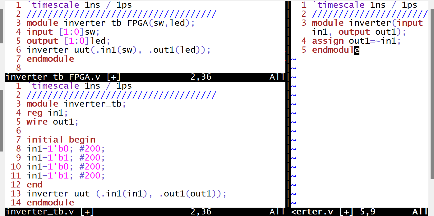
Inverter
The code shown in Figure 1.
includes three modules. The first module, "inverter," defines a
inverter which outputs the opposite of the input signal. The second
module, "inverter_tb," is the testbench for vivado simulation, setting
input values and observing the output. The third module,
"inverter_tb_FPGA," is designed for on-board logic testing.
Figure 1. Gvim code of inverter implementation
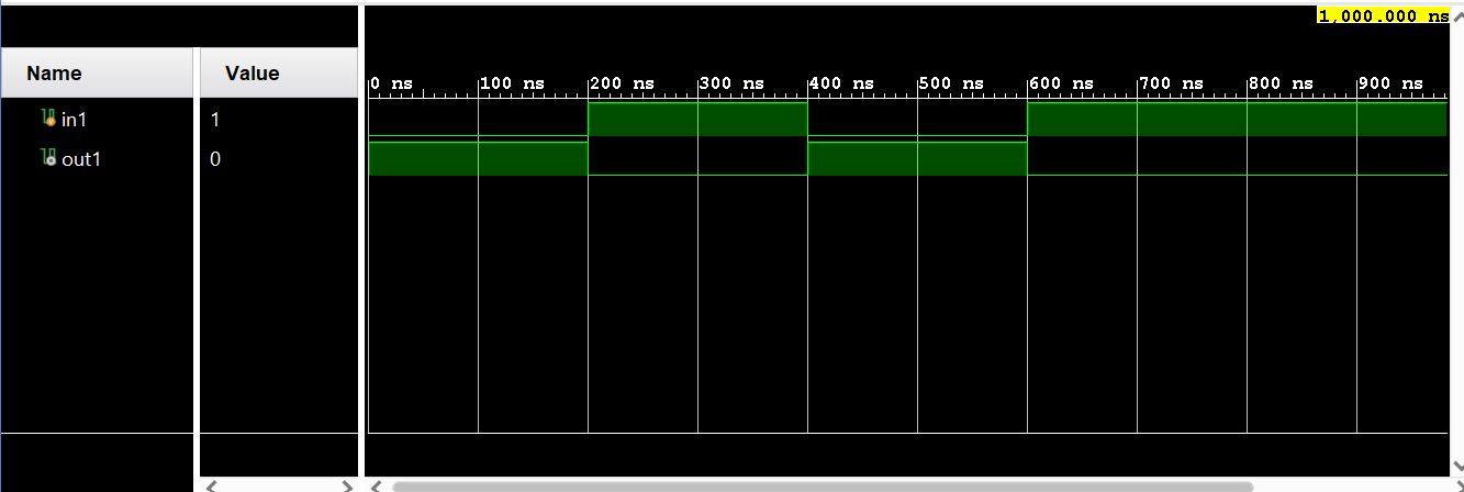
Figure 2. Vivado simulation of Inverter
Video 1. Demonstration of the inverter on the FPGA board
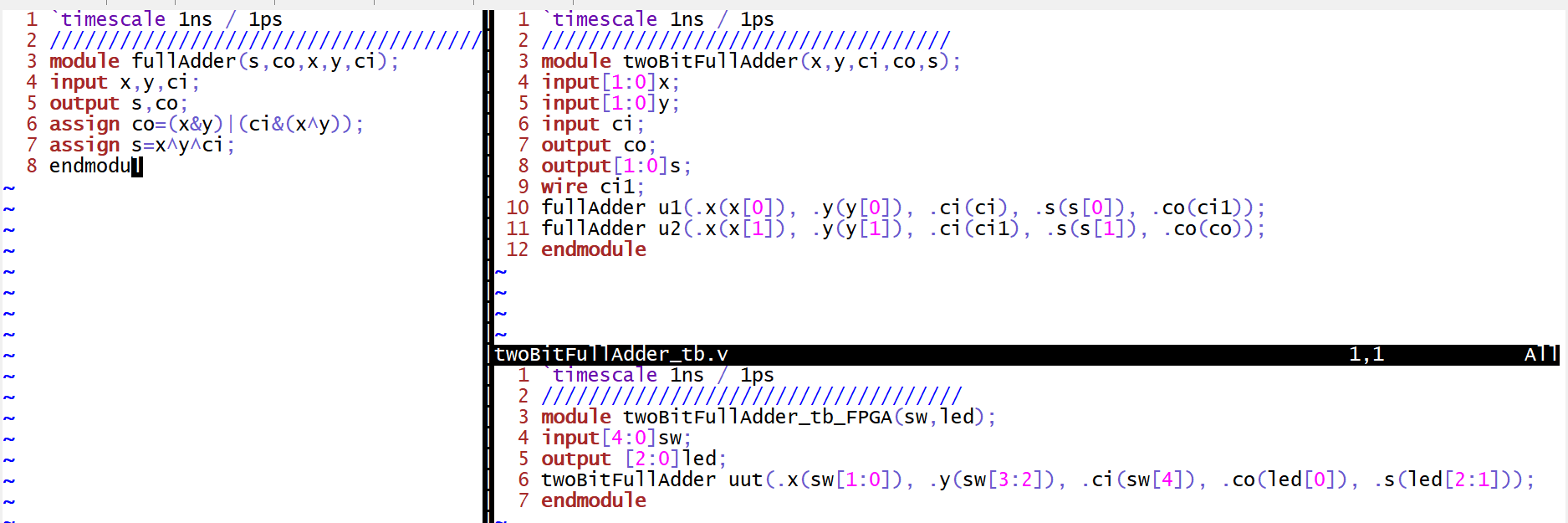
2-bit Full Adder
The code showed in Figure 3.
implements a two-bit full adder using modules for individual full
adders. The "fullAdder" module defines the logic for a 1-bit full
adder, and the "twoBitFullAdder" module utilizes two instances of this
module which is the testbench for the vivado simaltion. Input vectors
"x" and "y" represent the 2-bit binary numbers to be added, and "ci" is
the carry-in. The module outputs a sum "s" and carry-out "co". The
carry-out from the first full adder is connected to the second full
adder as the carry-in, demonstrating the 2-bit full adder. The third module, "twoBitFullAdder_tb_FPGA," is designed for FPGA on-board logic verification.
Figure 3. Gvim code of 2-bit Full Adder implementation
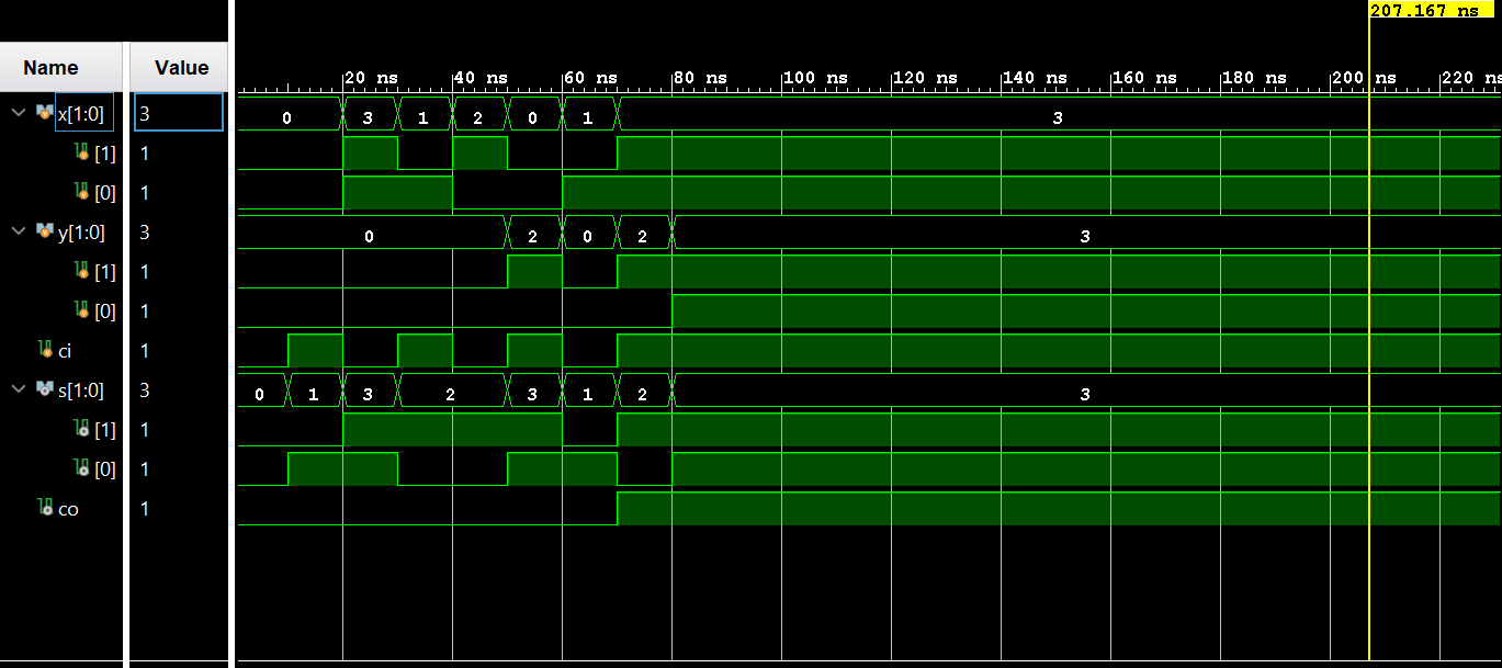
Figure 4. Vivado simulation of 2-bit Full Adder
Video 2. Demonstration of the 2-bit Full Adder on the FPGA board
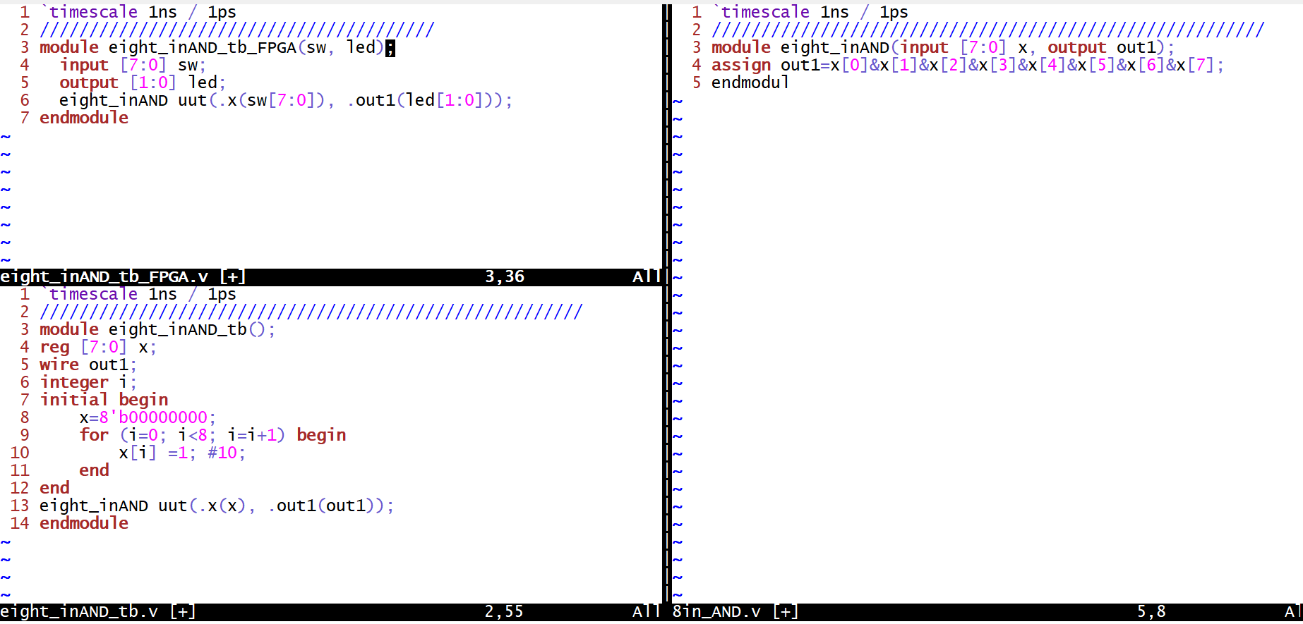
8-input AND gate
The code shown is Figure 5.
shows three modules. The first module, "eight_inAND," defines an
8-input AND gate, with inputs represented by the 8-bit vector "x" and
an output "out1" calculated as the logical AND of all input bits. The
second module, "eight_inAND_tb," is the testbench for vivado
simulation, initializing the input vector "x" with zeros and then
sequentially setting each bit to 1 with a 10-time unit delay. The third
module, "eight_inAND_tb_FPGA," is designed for FPGA on-board logic
verification.
Figure 5. Gvim code of 8-input AND gate implementation
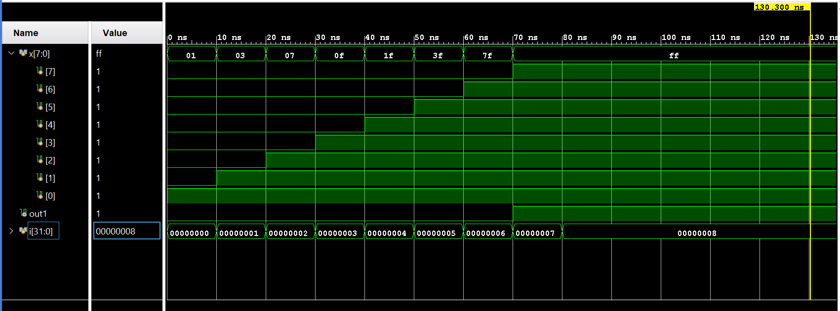
Figure 6. Vivado simulation of 8-input AND gate
Video 3. Demonstration of the 8-input AND gate on the FPGA board
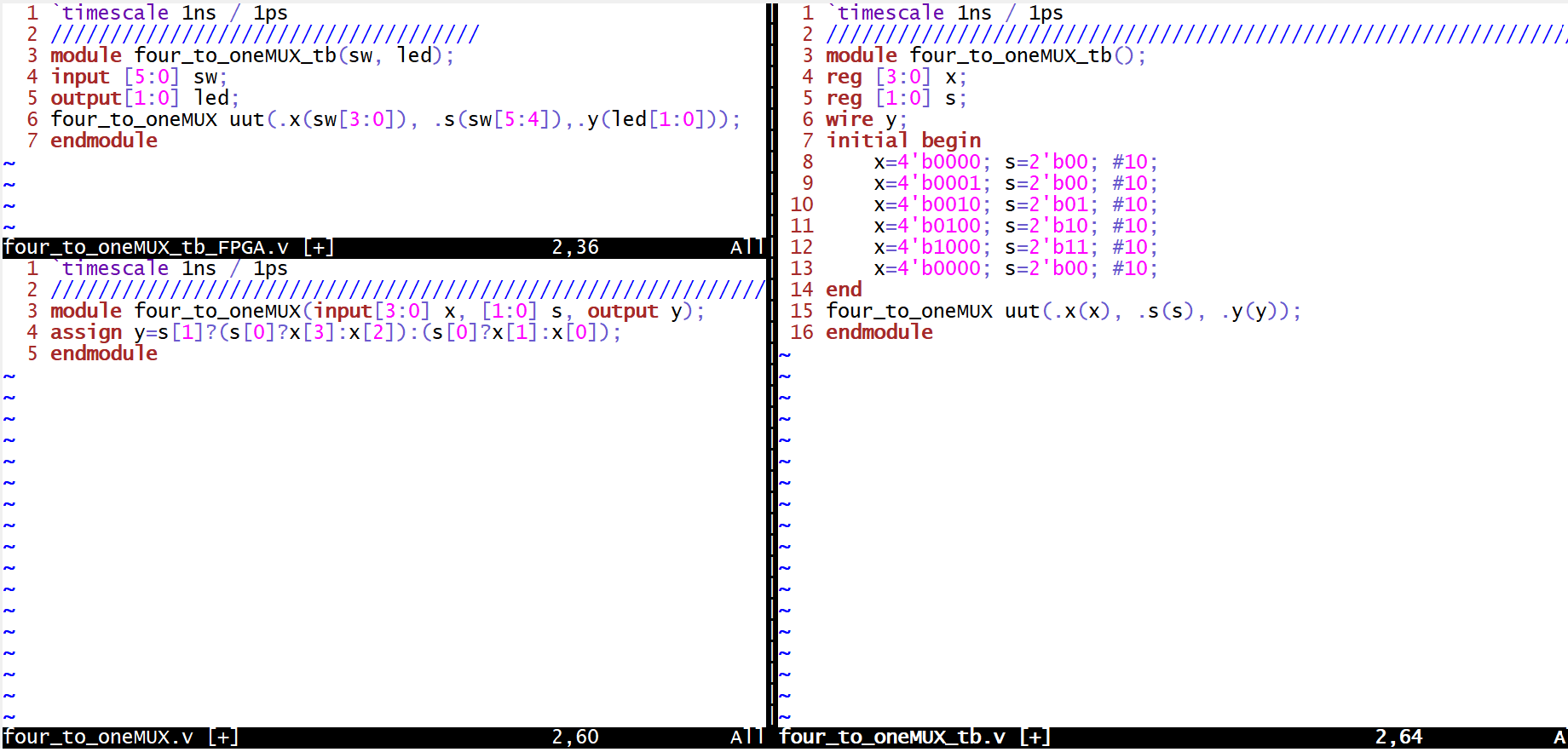
4-to-1 Multiplexer
The code shown in Figure 7.
comprises three modules. The first module, "four_to_oneMUX," defines a
4-to-1 multiplexer with inputs represented by the 4-bit vector "x", a
2-bit selection vector "s", and an output "y". The assignment for "y"
is based on the conditional expression using the selection vector "s".
The module on left top, is the testbench for FPGA testing, connecting a
6-bit switch input "sw" to the MUX and outputting a 2-bit signal "led".
The module on right is the testbench for the vivado simulation that
sequentially sets input "x" and selection vector "s" values, observing
the output "y" with a 10-time unit delay between each configuration
change.
Figure 7. Gvim code of 4-to-1 MUX implementation
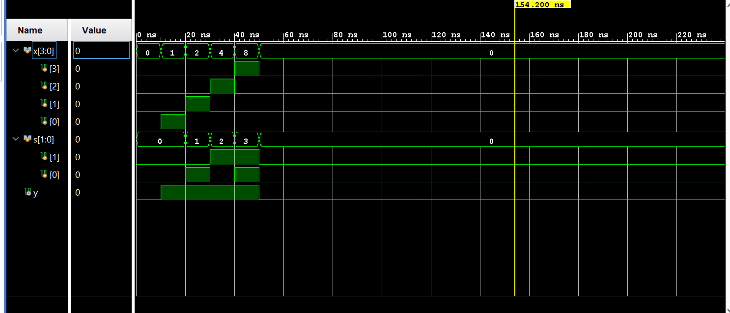
Figure 8. Vivado simulation of 4-to-1 MUX
Video 4. Demonstration of the 4-to-1 MUX on the FPGA board
Task 2: Complete the tasks in Section 2. Show your code, explanation, and demonstrate it in an embedded video.
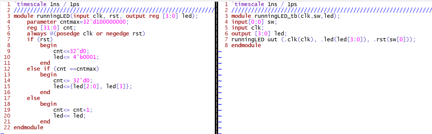
The code shown in Figure 9.
consists of two modules. In the "runningLED" module, a running LED
pattern is defined, controlled by a 32-bit counter. The LED pattern
shifts to the left when the counter reaches its maximum value. The
second module, "runningLED_tb," is the testbench, connecting inputs
"clk" and "sw" to the "runningLED" module and observing the 4-bit LED
output. The reset signal is derived from the least significant bit of
the switch input. This code demonstrates a simulation of the running
LED circuit at a second frequency.
Figure 9. Gvim code of four running LEDs implementation
Video 5. Demonstration of four running LEDs on the FPGA board
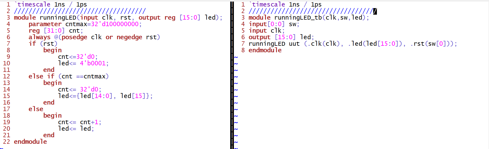
Task 3: Similar to the example in Section 2, show running LEDs on all
16 LEDs. Show your code, explanation, and demonstrate it in an embedded
video.
The code shown in Figure 10.
has the same modules as the code shown in Task 2 with a modification in
the utilized LEDs number. This version of the code uses 16 LEDs instead
of four.
Figure 10. Gvim code of all sixteen running LEDs implementation
Video 6. Demonstration of all sixteen running LEDs on the FPGA board
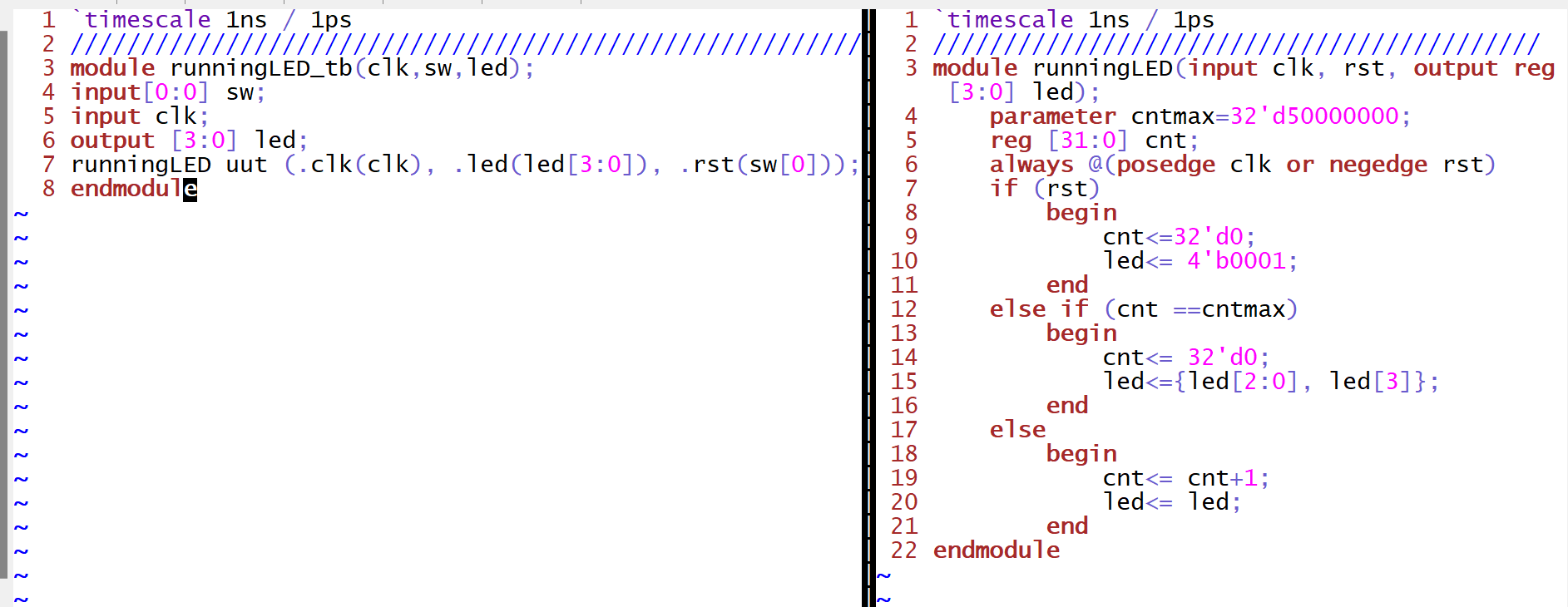
Task 4: Similar to the example in Section 2, change the frequency of
the 4 running LEDs to half second and demonstrate it in an embedded
video.
The code shown in Figure 11.
has the same modules as the code shown in Task 2 with a modification in
the frequency of the running LEDs . This version of the code has a frequency of half a second intead of one second.
Figure 11. Gvim code of four running LEDs with a faster speed implementation
Video 7. Demonstration of four running LEDs with a faster speed on the FPGA board
Task 5: Complete the task in Section 3. Show your code, explanation, and demonstrate it in an embedded video.
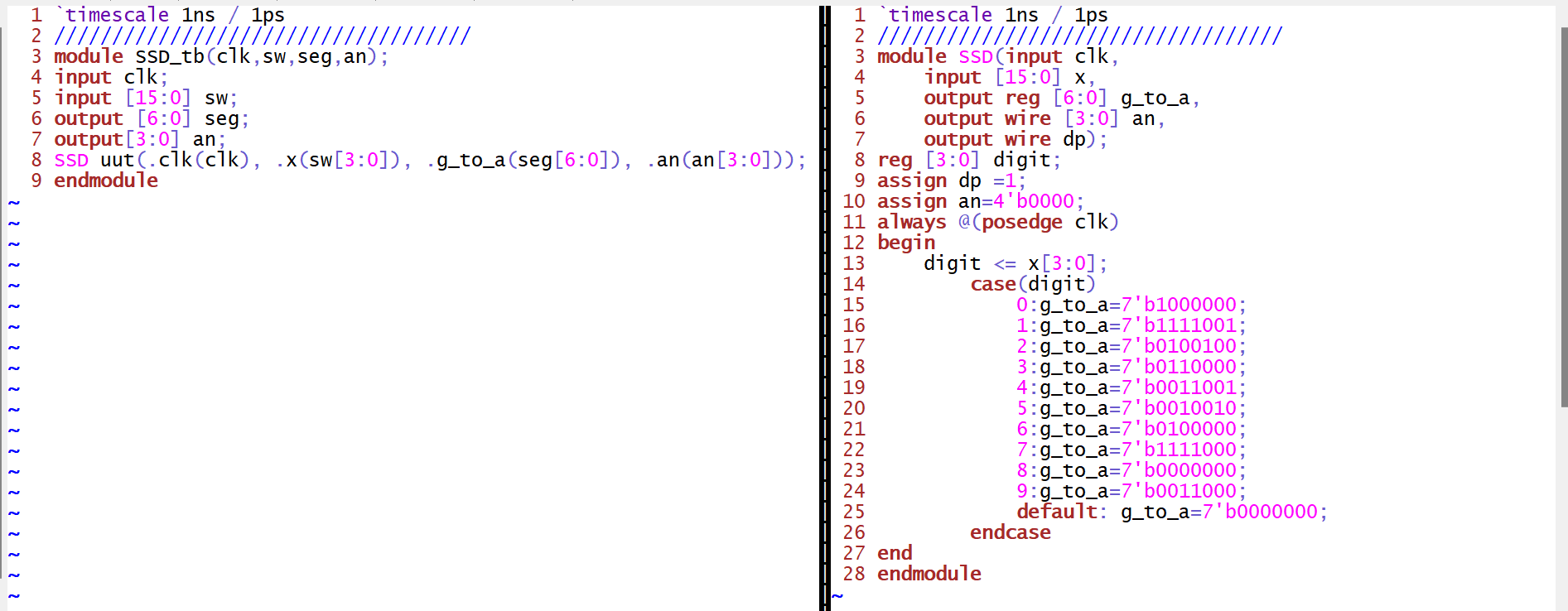
The "SSD" module shown in Figure 12. is a 4-digit 7-segment
display controller, taking inputs "clk" and "x", and outputting display
signals "g_to_a", digit select signals "n", and a decimal point signal
"dp". The display pattern is updated based on the lower 4 bits of the
input "x" on each clock edge. The "SSD_tb" is the testbench, connecting
inputs "clk" and "sw" to the "SSD" module and observing the 7-segment
display output "seg" and digit select output "an".
Figure 12. Gvim code of 7-segment display implementation
Video 8. Demonstration of 7-segment display on the FPGA board
WEEK 2:
Task 1: Complete the task in Section 4. Show your code, explanation, and demonstrate it in an embedded video.
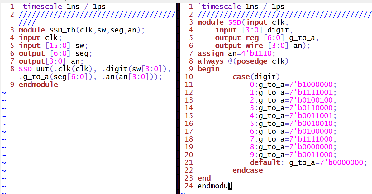
The modified "SSD" module is designed to control a 7-segment display
"seg" based on the input clock signal "clk" and the 4-bit input digit
sw[3:0]. It uses a case statement to assign specific patterns to the 7
segments "g_to_a" depending on the digit value. It disables the first 3
of the 7- segment displays and displays the counter on the most right
7- segment display.
Figure 13. Gvim code of modified 7-segment display implementation
Video 9. Demonstration of modified 7-segment display on the FPGA board
Task 2: Show "FLC" on three of the display units. Show your code, explanation, and demonstrate it in an embedded video.
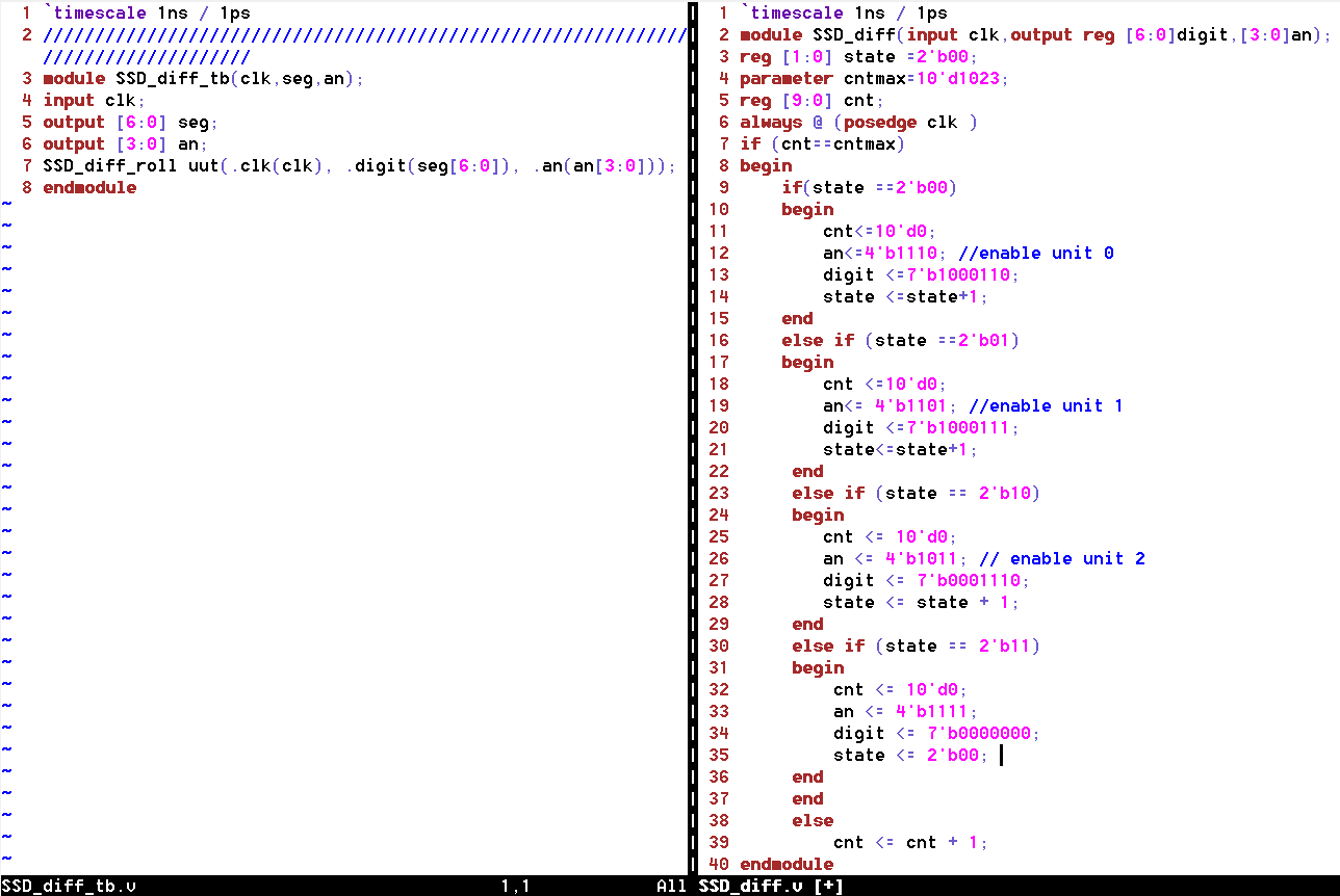
The "SSD_diff" module shown in Figure 14.
utilizes a clock signal "clk" to control the display, counting through
different states to enable each digit and display specific pattern
"FLC". The "SSD_diff_tb" is the testbench. The "clk" input controls the
timing, while the "seg" and "an" outputs represent the 7-segment
display segments and digit enable signals, respectively.
Figure 14. Gvim code of displaying FLC on the display units implementation
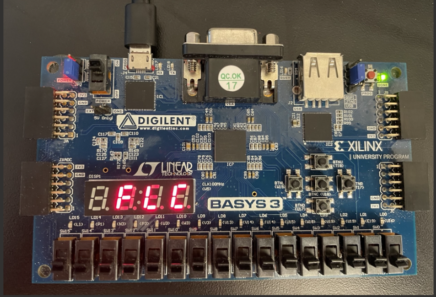
Figure 15. Demonstration of displaying FLC on the display unit on the FPGA board
Task 3: Roll "FLC" to the left for every half second. After "F" shifted
out to the left, it should appear on the right hand side. Show your
code, explanation, and demonstrate it in an embedded video.
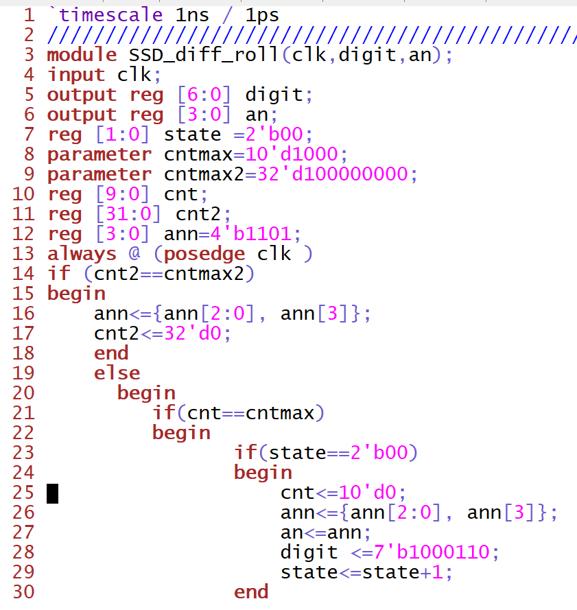
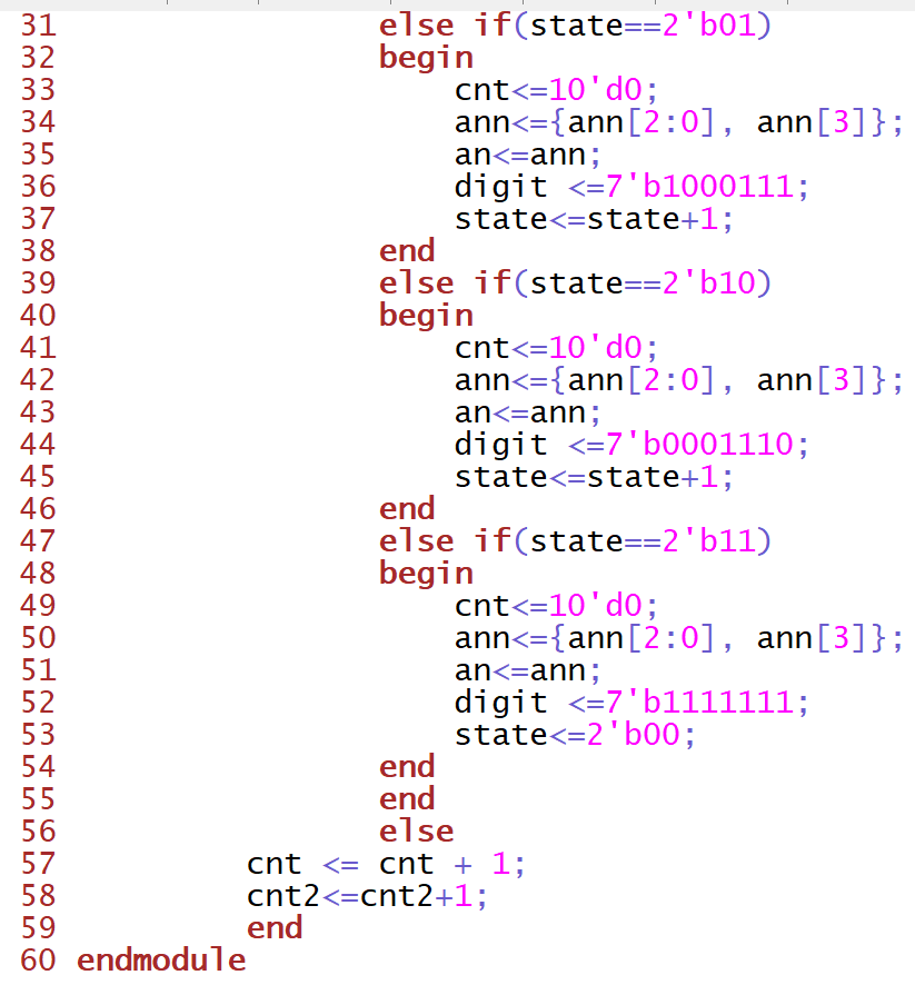
The "SSD_diff_roll" module shown in Figure 16. is similarly to the code shown in Figure 14. uses a clock signal to counting through different states to display "FLC."
Additionally, there is a rolling effect implemented by shifting the
digit enable signals "an" in the "ann" variable to shift the pattern to
the left. The same testbench shown in Figure 14. also used in this implementation.
Figure 16. Gvim code of displaying FLC and shifting to the left on the display units implementation
Video 10. Demonstration of displaying FLC shifting to the left on the display unit on the FPGA board
Discussion: In conclusion, this lab provided hands-on
experience with Verilog and FPGA programming, covering fundamental
digital circuits and applications. We implementing inverters, adders,
multiplexers, a running LED program, and a 4-digit 7-segment display
controller. We gained practical insights into hardware languages and
FPGA development. Overall, I think this lab strengthened our skills in
Verilog and Vivado and deepened our understanding of digital system
designs.