CE 433 Spring 2024 Homework 3: Combinational Logic Block Sahra Genc sggenc@fortlewis.edu LAB 3:Combinational Logic Blocks
Task 1: Repeat the
simulation of Half Adder and Full Adder in Section 1. Show the code,
code explanations, and simulation results in your report.
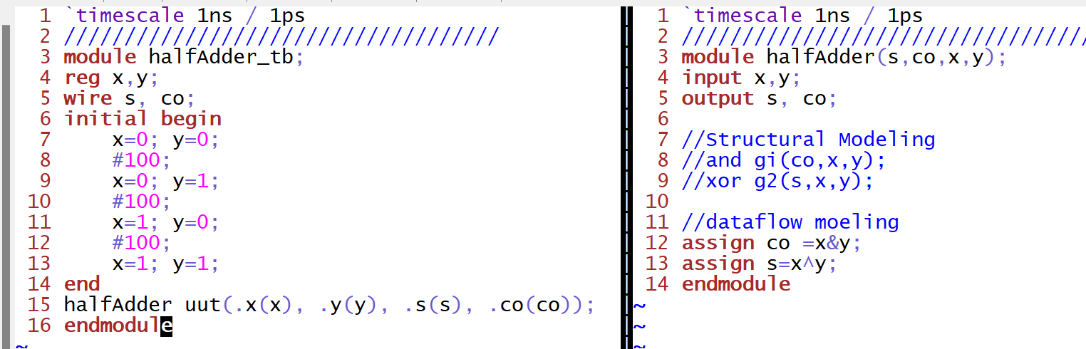
The code shown in Figure 1.
computes the sum output "sum" using an XOR gate, representing the
addition of the two input bits from "s". The carry-out "cout" is
determined by an AND gate based on the input bits. The "halfadder_tb"
is the testbench, setting different input combinations "x" and "y"
and observing the corresponding outputs "s" and "co" after specified
delays.
Figure 1. Gvim code of the half adder implementation
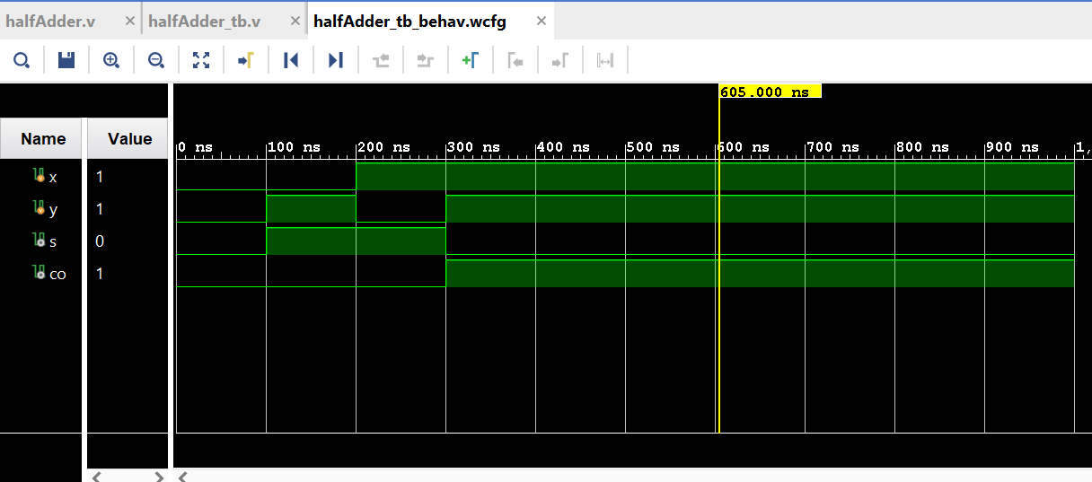
Figure 2. Vivado simulation of the half adder
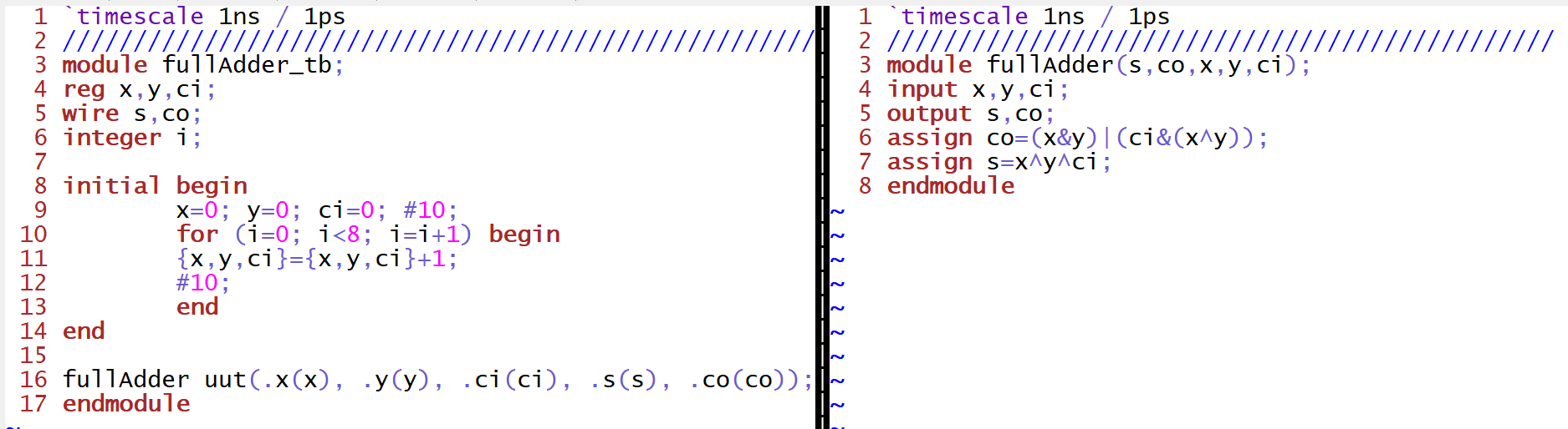
The shown code in Figure 3.
calculates the out put "sum" using XOR gates, representing the addition
of three inputs: the two bits from "s" and the carry-in "cin". The
carry-out "cout" is determined through a combination of AND and OR
gates based on the input bits. The "fulladder_tb" is the testbench, initializing inputs and observing outputs after delays. A loop
simulates eight input combinations to test the "fullAdder"
module functionality.
Figure 3. Gvim code of the full adder implementation
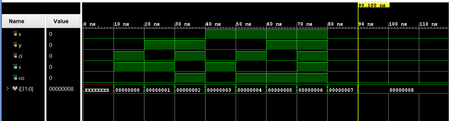
Figure 4. Vivado simulation of the full adder
Task 2: Design the testbench for the comparator in Section 2. Show the
code, code explanations, and simulation results in your report.
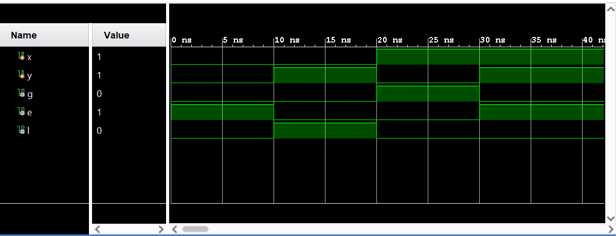
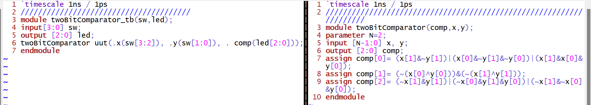
The "twoBitComparator" module shown in Figure 5.
implements a 2-bit binary comparator, generating three outputs "g",
"e", "l" indicating whether the first number is greater, equal, or less
than the second. The "twoBitComparator_tb" is the testbench, cycling
through different 2-bit input combinations "x" and "y" with a 10-time
unit delay between each set of inputs.
Figure 5. Gvim code of the 2-bit Comaparator implementation
Figure 6. Vivado simulation of the 2-bit Comaparator
Task 3: Design the testbench for the 4-bit comparator in Section 3.
Show the code, code explanations, and simulation results in your
report.
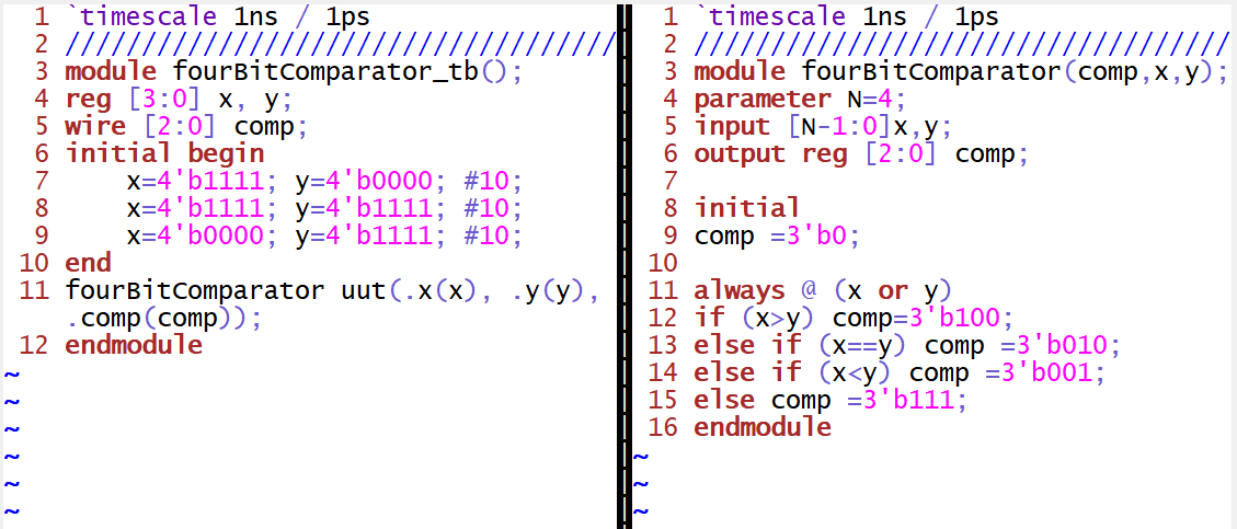
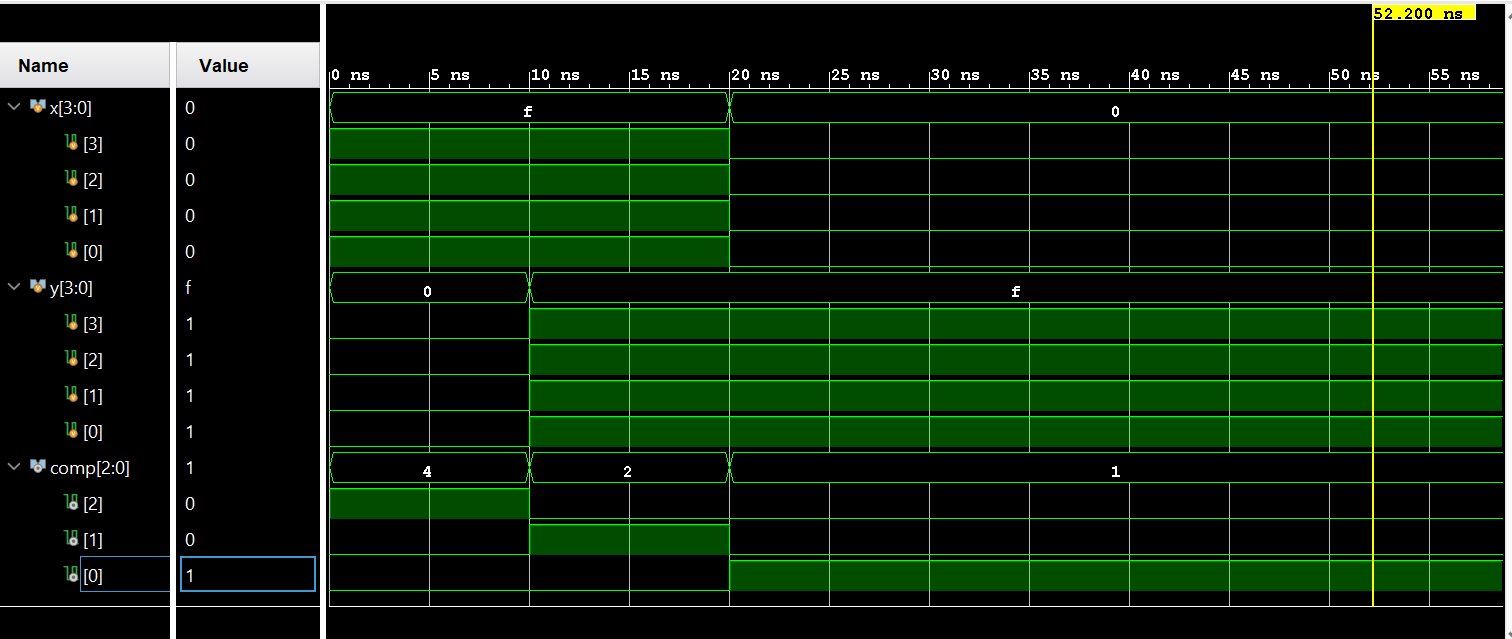
The "fourBitComparator" module shown in Figure 7.
implements a 4-bit magnitude comparator, comparing two 4-bit inputs "x"
and "y". The 3-bit output "comp" indicates whether "x" is greater,
equal, or less than "y". The "fourBitComparator_tb" is the testbench,
initializing the 4-bit inputs with different combinations and observing
the 3-bit output "comp" after a 10-time unit delay between each set of
inputs.
Figure 7. Gvim code of the 4-bit Comaparator implementation
Figure 8. Vivado simulation of the 4-bit Comaparator
Task 4: Implement a 2-bit comparator on the Basys 3 board. Use sw as
inputs and led as outputs. Show the code, code explanations, and an
embedded Youtube video demonstration in your report.
The "twoBitComparator" module shown in Figure 9.
implements a two-bit binary comparator, producing a 3-bit result "comp"
indicating greater-than, equal-to, and less-than conditions between two
2-bit binary numbers "x" and "y". The "twoBitComparator_tb" module is
testbench, connecting a 4-bit switch input "sw" to the comparator and
displaying the 3-bit result on LED outputs "led".
Figure 9. Gvim code of the 2-bit Comaparator implementation
Video 1. Demonstration of the 2-bit Comaparator on FPGA board
Task 5: In Section 4, design the testbench for the decoder and verify
the logic in simulation (use the Dataflow modeling method). Show the
code, code explanations, and simulation results in your report.
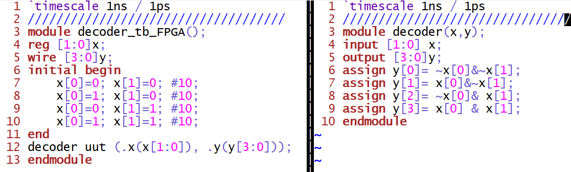
The "decoder" module shown in Figure 10.
implements a 2-to-4 decoder, generating a 4-bit output "y" based on the
2-bit input "x". Each bit in "y" corresponds to a specific binary
combination of the input bits. The "decoder_tb_FPGA" is the testbench,
cycling through different input combinations "x" with a 10-time unit
delay between each set.
Figure 10. Gvim code of the decoder implementation
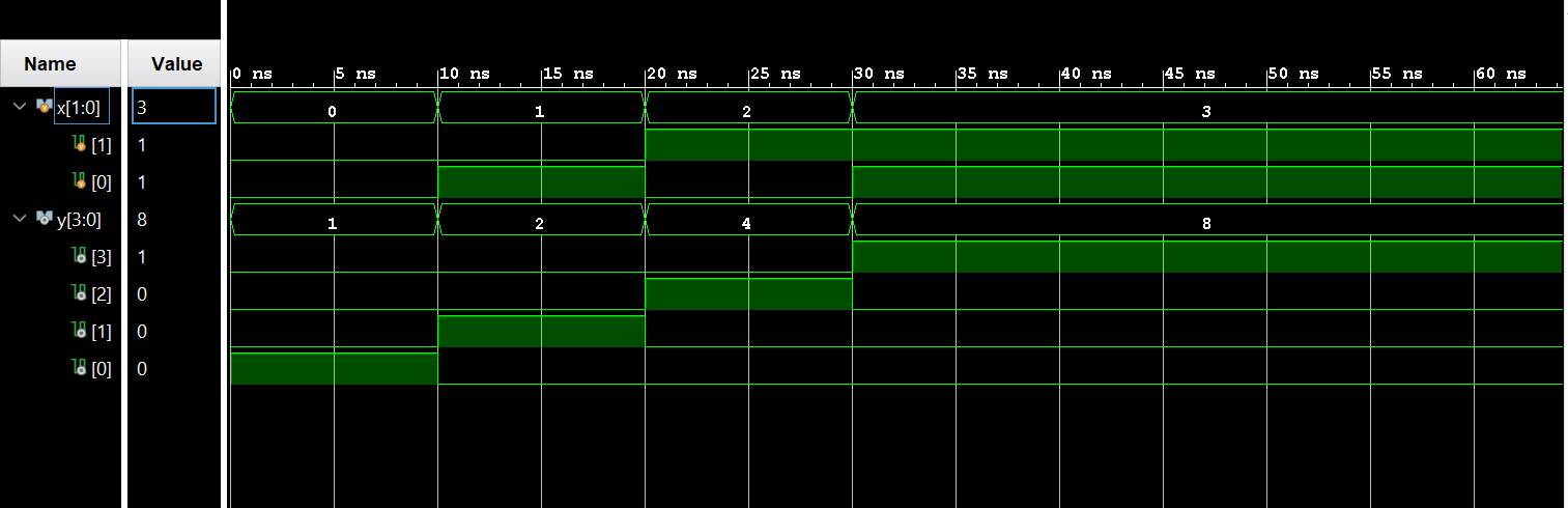
Figure 11. Vivado simulation of the decoder
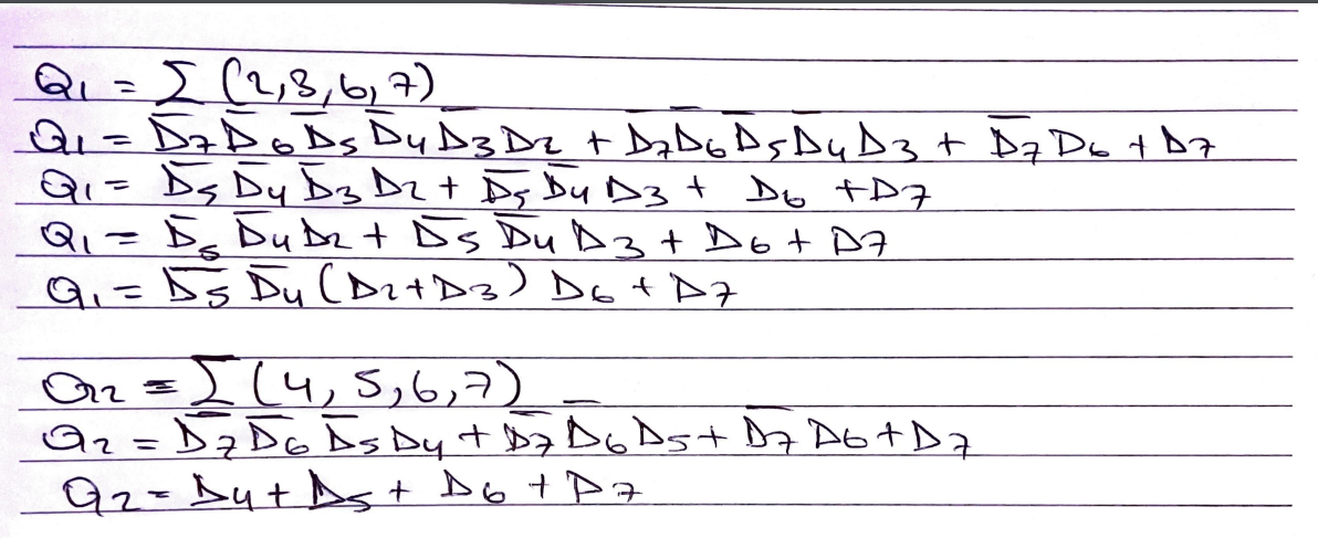
Task 6: In Section 5, for the 8x3 priority encoder, find Q2 and Q1,
build the module and verify the logic using simulations. Show the code,
code explanations, and simulation results in your report.
Figure 12. Logic derivation of Q2 and Q1
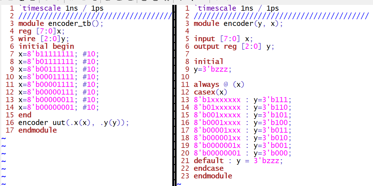
The "encoder" module shown in Figure 13.
implements an 8-to-3 priority encoder, where the output "y" encodes the
highest-order active bit position in the 8-bit input "x". The
"encoder_tb" module serves as a testbench, initializing the 8-bit input
with different combinations and observing the 3-bit output "y" after a
10-time unit delay between each set of inputs.
Figure 13. Gvim code of the 8x3 priority encoder implementation
Figure 14. Vivado simulation of the 8x3 priority encoder
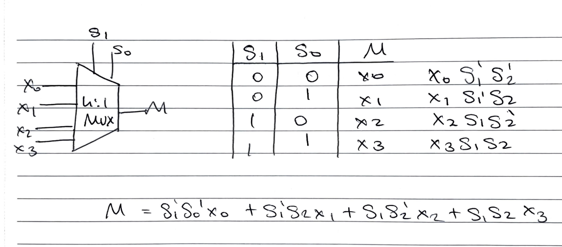
Task 7: Derive the logic expression of a 4-1 multiplexer. Show the process on a paper, insert it as an image into your report.
Figure 15. Logic derivation of 4-1 multiplexer
Task 8: In Section 6, implement a 4-1 multiplexer on your Basys 3
board. Show the code, code explanations, and an embedded Youtube video
demonstration in your report.
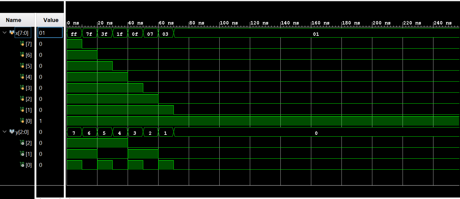
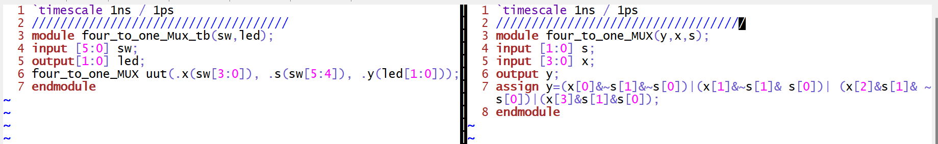
The "four_to_one_MUX" module shown in Figure 16.
implements a 4-to-1 multiplexer, where the output "y" is determined by
the select inputs "s" and the 4-bit input "x". The "four_to_one_Mux_tb"
module serves as a testbench, connecting a 6-bit switch input "sw" to
the multiplexer and observing the 2-bit output on LED outputs "led".
Figure 16. Gvim code of the 4-1 multiplexer implementation
Video 2. Demonstration of the 4-1 multiplexer on FPGA board
Task 9: Design/verify an even parity generator and checker in
simulation respectively. Implement an even parity checker on your Basys
3 board - use sw as inputs, use leds as output indicators. Show the
code, code explanations, and an embedded Youtube video demonstration in
your report.
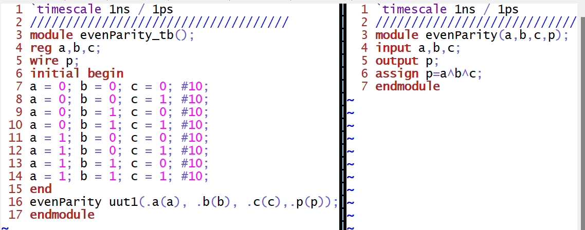
The "evenParity" module shown in Figure 17.
defines an even parity checker, where the output "p" is the result of
an XOR operation on inputs "a", "b", and "c". The "evenParity_tb"
module is the testbench for the simlation, It is applying different
combinations of inputs "a", "b", "c" and observing the output "p" after
a 10-time unit delay for each combination.
Figure 17. Gvim code of the even parity generator implementation
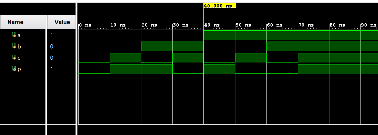
Figure 18. Vivado simulation of the even parity generator
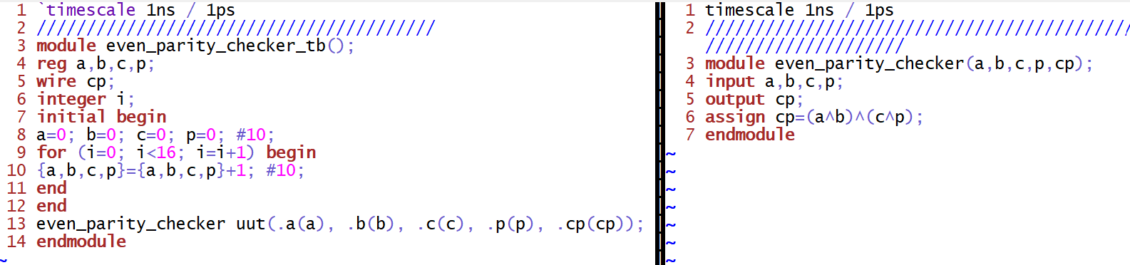
The
first module, "even_parity_checker_tb," shown in Figure 19. is the testbench for the simaltion. It
initializes input variables "a", "b", "c", and "p" to 0 and observes
the output "cp" after a delay. Subsequently, it increments these inputs
in a loop to simulate various input combinations. The second module,
"even_parity_checker," defines an even parity checker circuit with
inputs "a", "b", "c", and "p", and output "cp". The output "cp" is
determined by XOR pairs of input bits.
Figure 19. Gvim code of the even parity checker implementation
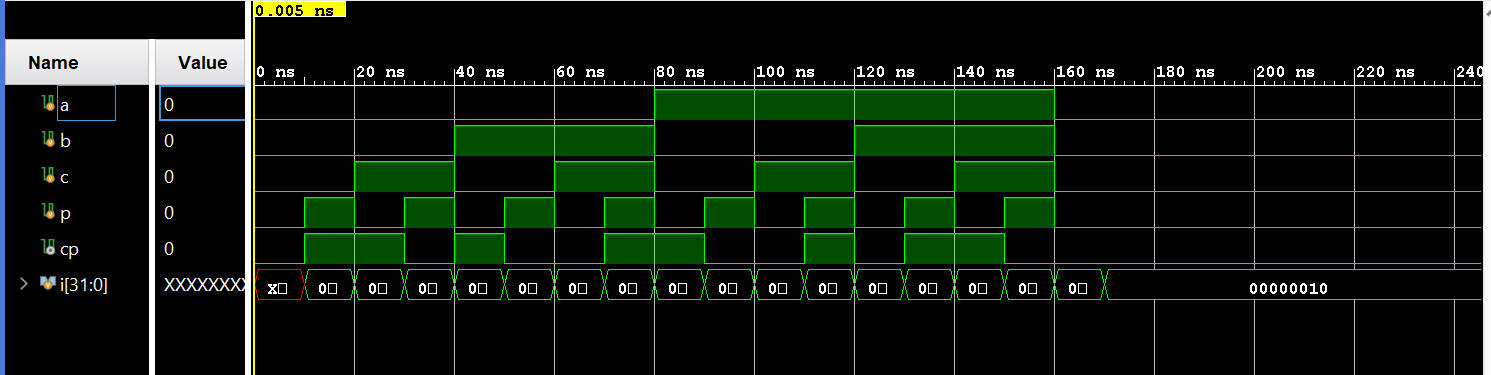
Figure 20. Vivado simulation of the even parity checker
Video 3. Demonstration of the even parity checker on the FPGA board
Task 10: Implement the design in Section 8 and Section 9 on your Basys
3 board. Show embedded Youtube video demonstration on your report. Show
the code, code explanations, and an embedded Youtube video
demonstration in your report.
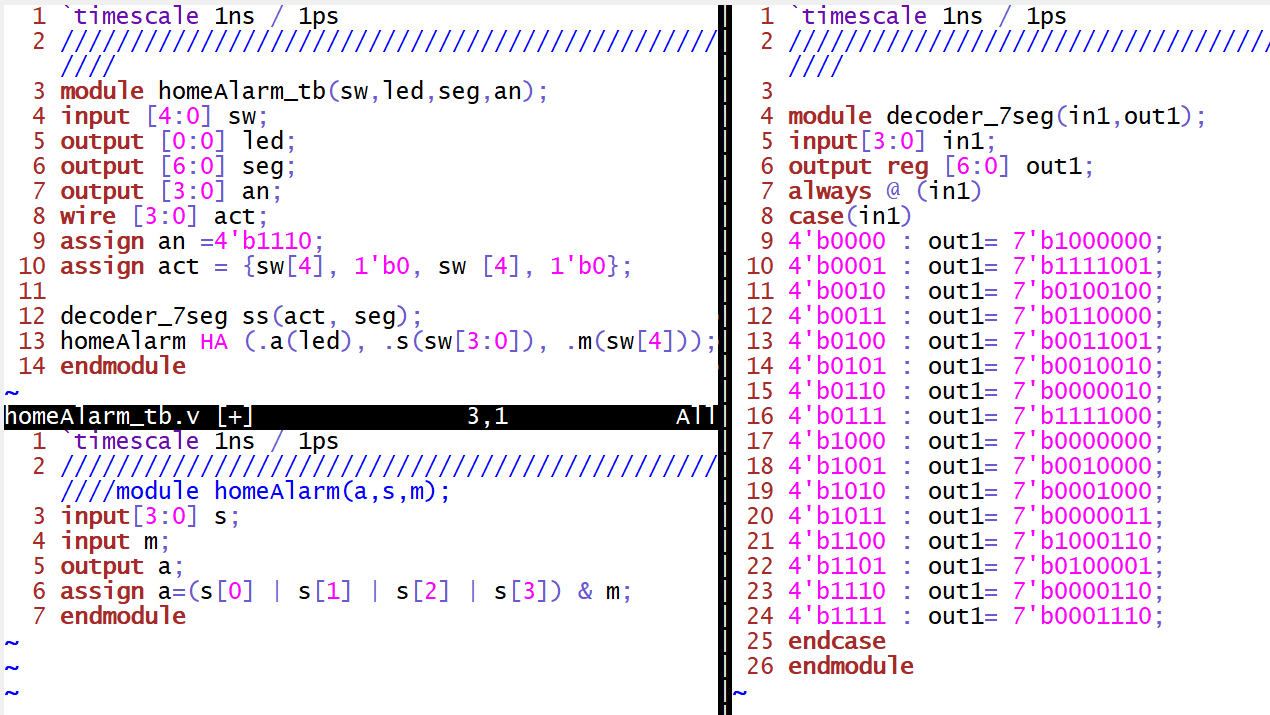
The "homeAlarm" module shown in Figure 21.
defines a home alarm system where the activation signal "a" is
generated if any of the four sensors "s" is triggered, and the switch
"m" is enabled. The "homeAlarm_tb" is the testbench, simulating the
alarm activation by assigning a specific pattern to the "act" wire
based on the switch input. The "decoder_7seg" module decodes the
pattern for visualization on a 7-segment display "seg".
Figure 21. Gvim code of the improved home alarm system implementation
Video 4. Demonstration of the improved home alarm system on the FPGA board
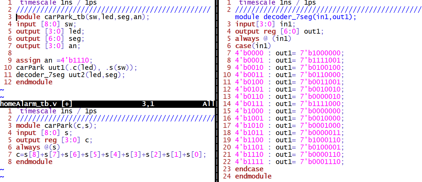
The "carPark" module shown in Figure 22.
functions as a car parking counter, summing the bits of a 9-bit switch
input "s" to represent the total number of cars. The testbench is
connecting the switch input to the car parking counter and observing
the 4-bit LED output "led" and the 7-segment display output "seg". The
"decoder_7seg" module decodes the LED pattern into a 7-segment display
format.
Figure 22. Gvim code of the improved counter with SSD implementation
Video 5. Demonstration of the improved counter with SSD on the FPGA board