CE 433 Spring 2024
Homework 1: Verilog and FPGA Basics
Sahra Genc
sggenc@fortlewis.edu
HOMEWORK 1: Verilog and FPGA Basics
Task 1: Use
gvim and Vivado to simulate the examples in section 2.1, 2.2, and 2.3.
Post snapshots of gvim windows and vivado simulation results in your
report. You must create testbenches for your simulations.

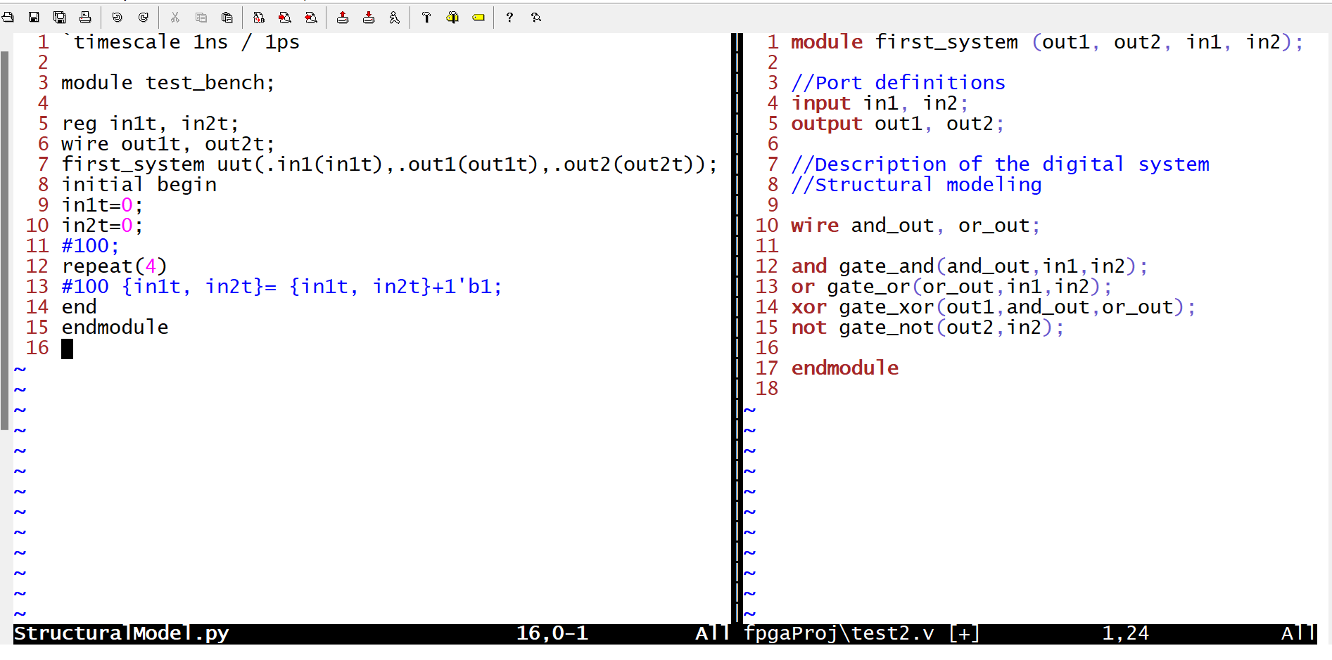
Figure 1. Snapshot of gvim windows of the example in section 2.1 (structural modeling)
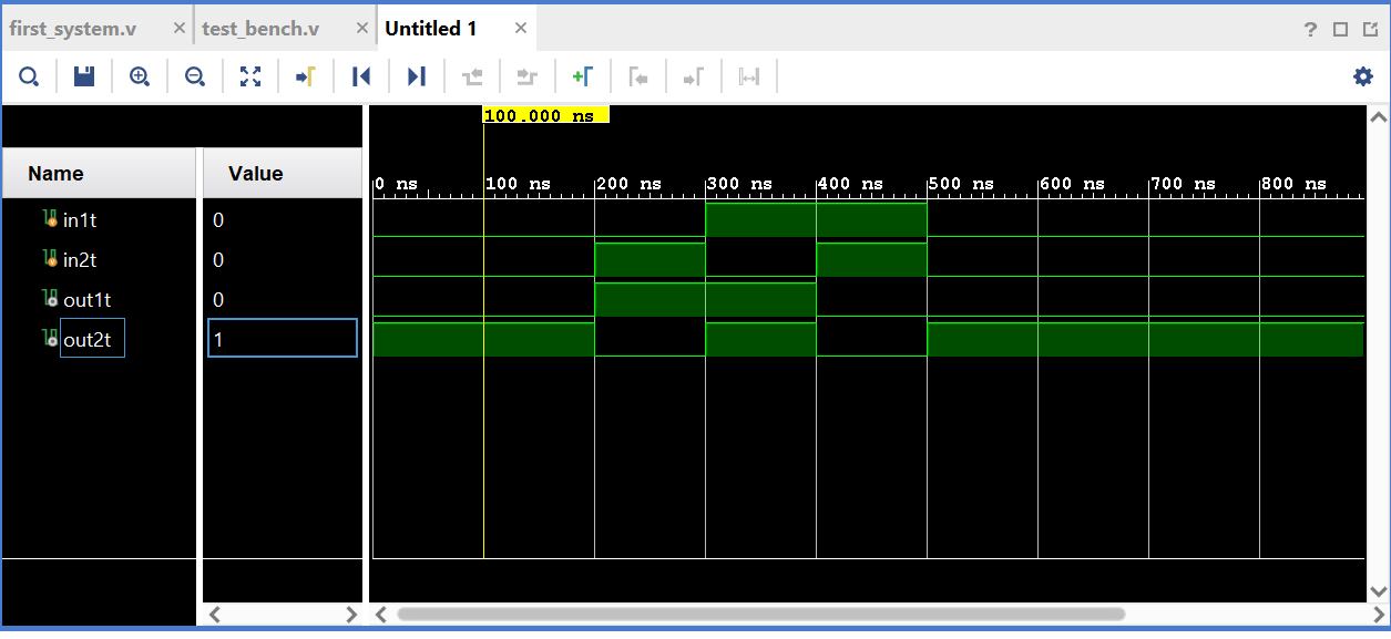
Figure 2. Snapshot of vivado simulation of the example in section 2.1 (structural modeling)
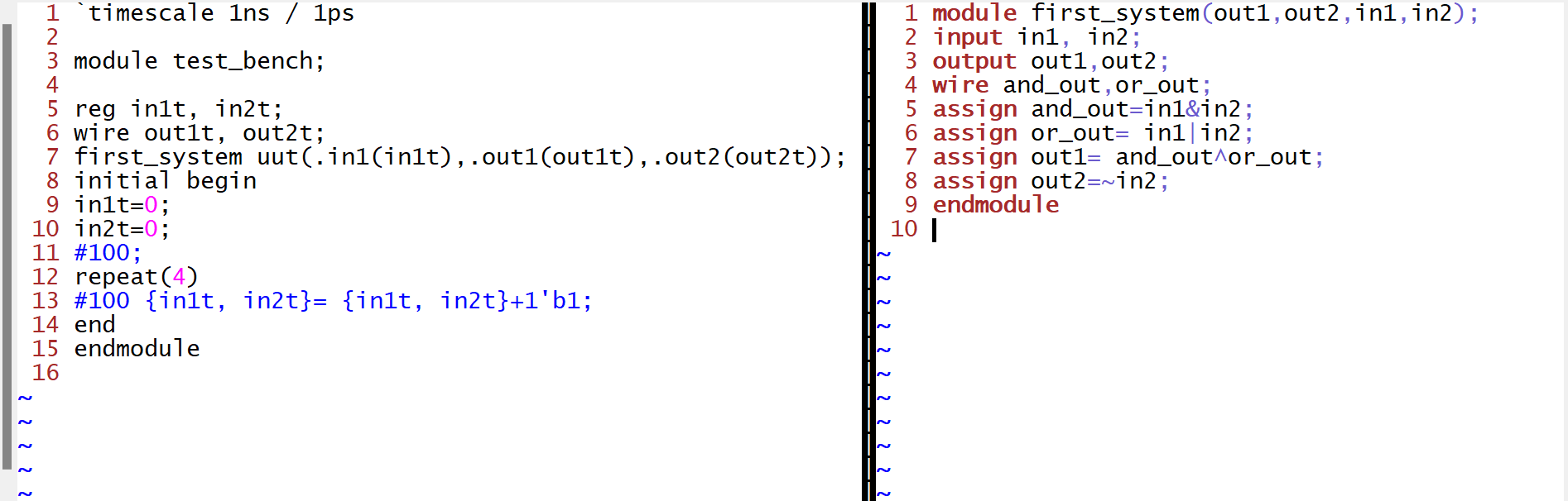
Figure 3. Snapshot of gvim windows of the example in section 2.2 (data flow modeling)
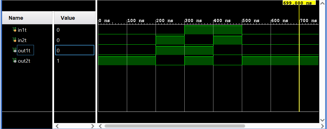
Figure 4. Snapshot of vivado simulation of the example in section 2.2 (data flow modeling)
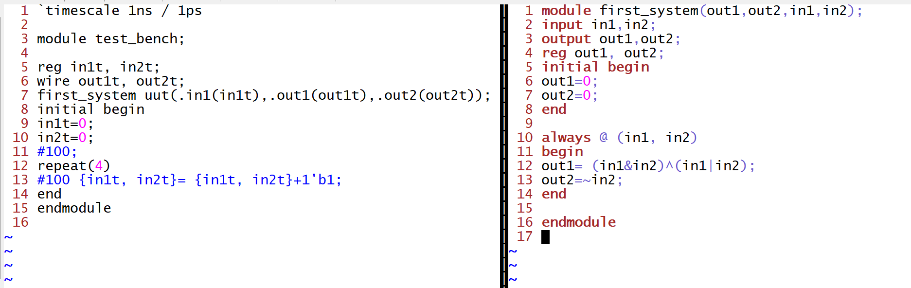
Figure 5. Snapshot of gvim windows of the example in section 2.3 (behavioral modeling)
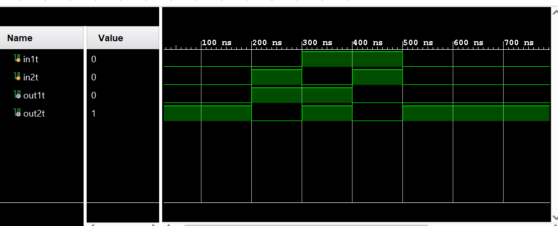
Figure 6. Snapshot of vivado simulation of the example in section 2.3 (behavioral modeling)
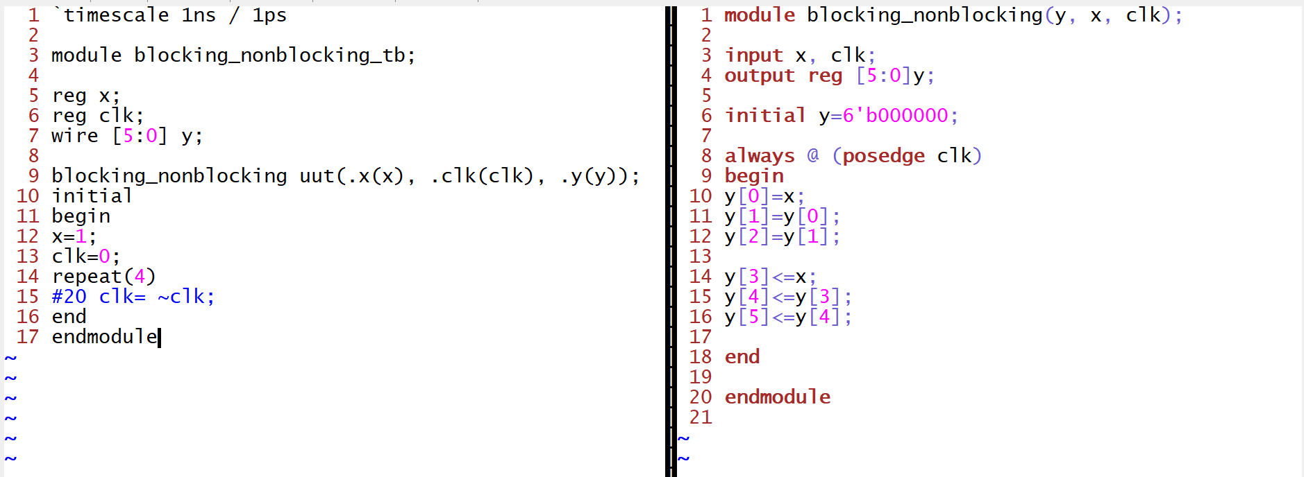 Figure 7. Snapshot of gvim windows of example in section 2.4
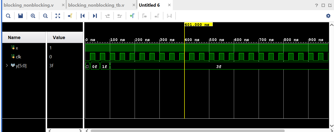
Figure 8.Snapshot of vivado simulation of the example in section 2.4
Task 3: Repeat the simulation example in 2.5.
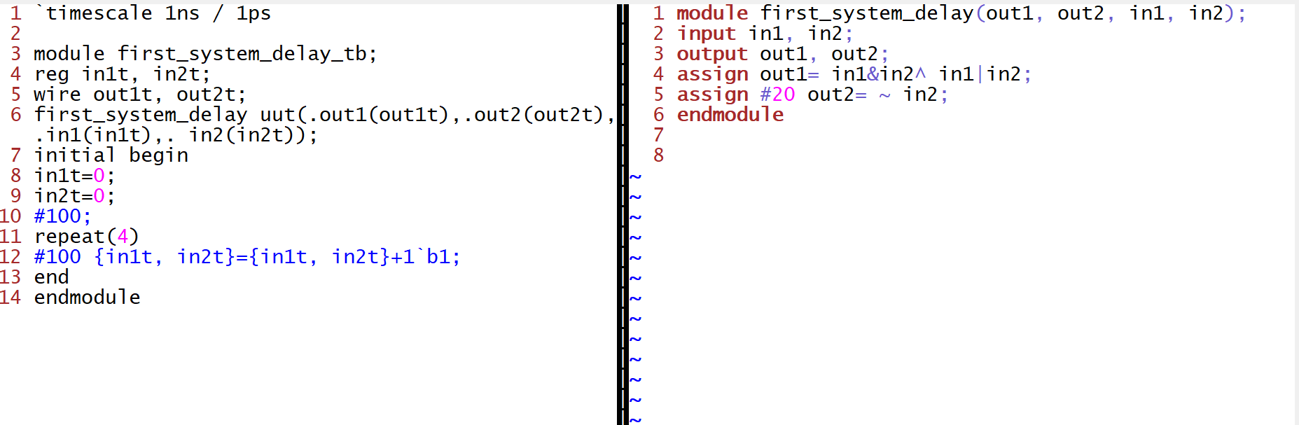 Figure 9. Snapshot of gvim windows of the example in section 2.5

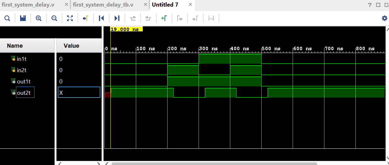 Figure 10. Snapshot of vivado simulation of the example in section 2.5
Task 4: For the example in section 2.5, move the 20 ns delay from Line 25 to Line 24 and run the simulation.
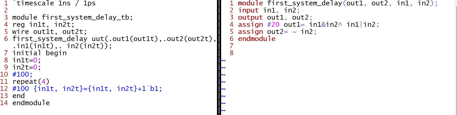 Figure 11. Snapshot of gvim windows of the example in section 2.5 (20ns delay moved to 4th line)
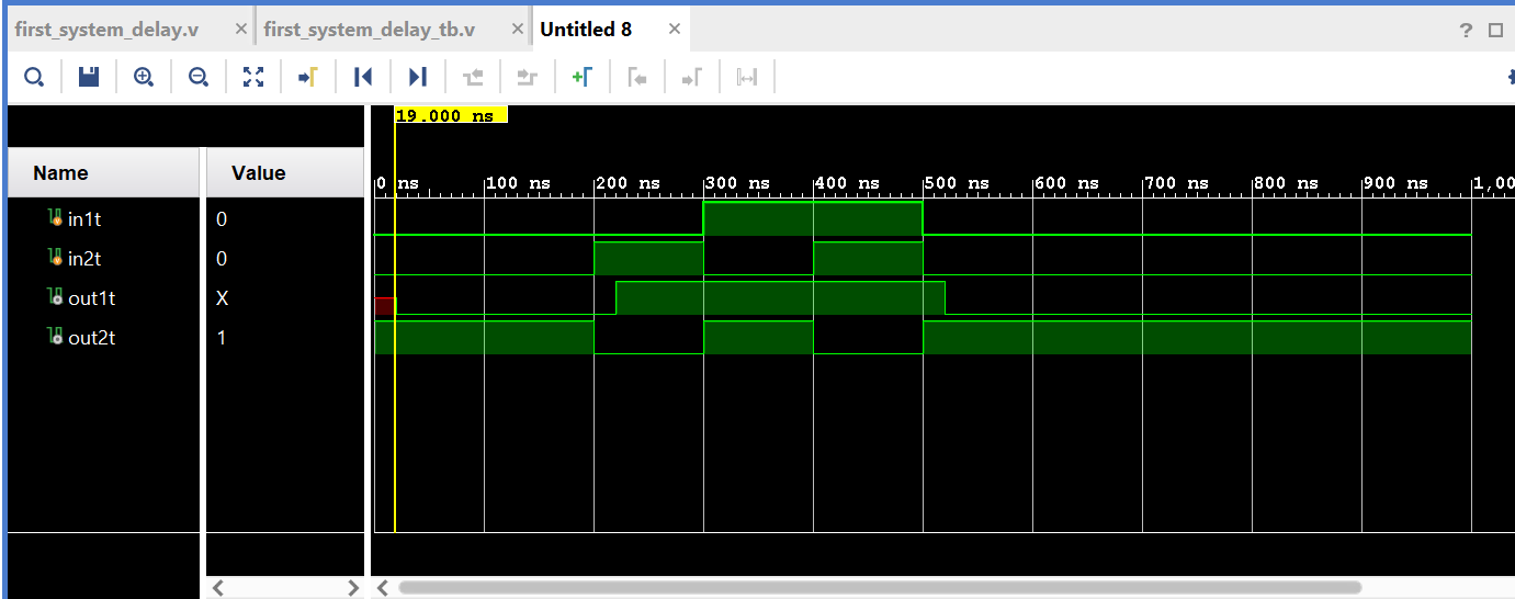 Figure 12. Snapshot of vivado simulation of the example in section 2.5 (20 ns delay moved to 4th line)
 Figure 13. Hand drawing of the time diagram
Task 6: Use gvim and vivado, repeat the example in section 2.6. Post the gvim windows and the vivado simulation windows for credit.
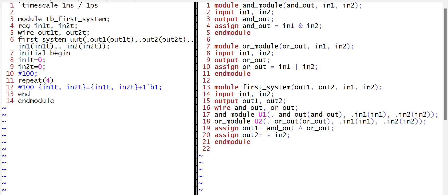 Figure 14. Snapshot of gvim windows of the example in section 2.6
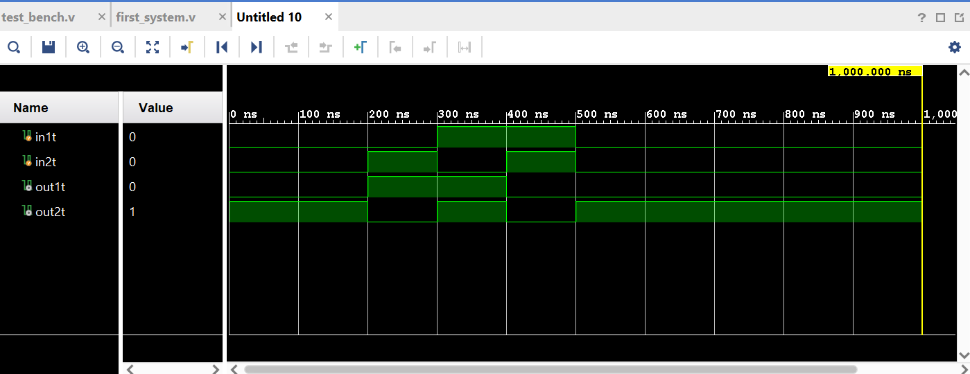 Figure 15. Snapshot of vivado simulation of the example in section 2.6