CE 433 Spring 2024 Final Prject : ADC and SPI Sahra Genc sggenc@fortlewis.edu
Final Project : ADC and SPI
Task : Replace the analog
amplifier with a potentiometer. First, connect the output of the
potentiometer to an Analog-to-Digital Converter (ADC) to digitize the
analog signal. Then, interface the digital output from the ADC to the
Serial Peripheral Interface (SPI) port input. Include a 5V/3.3V level
shifter between the Basys3 and the Arduino SPI ports to ensure
compatibility. Finally, configure the Arduino to transmit the digital
signal data to the serial monitor for display.
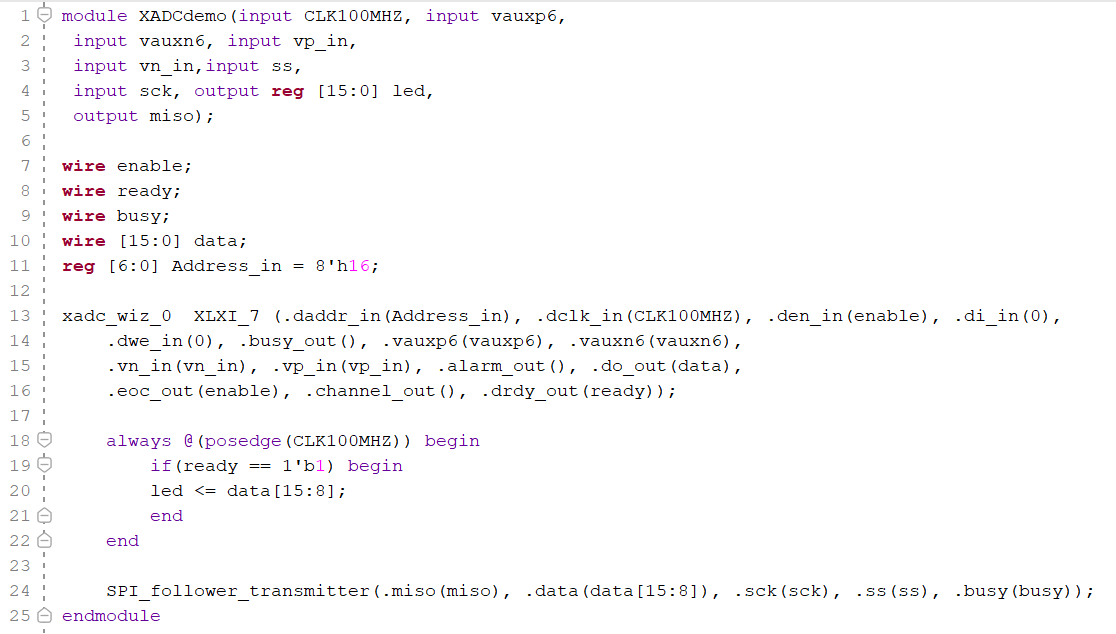
The Verilog module "XADCdemo" converts analog-to-digital and digital
communication. It integrates an XADC (Xilinx Analog-to-Digital
Converter) for converting analog signals from specific input pins and
an SPI (Serial Peripheral Interface) for data transmission. The module
is clocked by a 100 MHz signal and includes various inputs for analog
signals and SPI control. Within the module, an XADC converts the analog
inputs to digital format, outputting the data to a 16-bit register.
This data is displayed on LEDs and partially sent out through the SPI’s
MISO line by a SPI follower transmitter, which transmits only the 8
most significant bits of the ADC data. The continuous conversion
feature is enabled by looping the end of conversion signal back to the
conversion enable input, ensuring the XADC is consistently sampling and
updating the data.
Figure 1. The top module for ADC
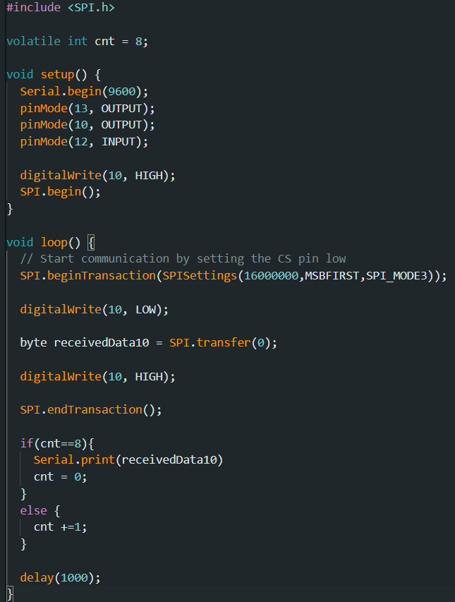
The Verilog module
"SPI_follower_transmitter" functions as an SPI slave transmitter, it
manages the transmission of an 8-bit data set to an SPI master. It
operates under a simple state machine with three states: Ready (RDY),
Transmit (TRANSMIT), and Stop (STOP). Triggered on the negative edge of
the SPI clock (sck), the module begins transmitting data when the Slave
Select (ss) line is active. It sequentially sends the data bits from
most to least significant, indicating busy status during transmission,
and resets upon completion. This design ensures synchronization with
the SPI clock and responsiveness to control signals.
Figure 2. SPI follower transmitter code
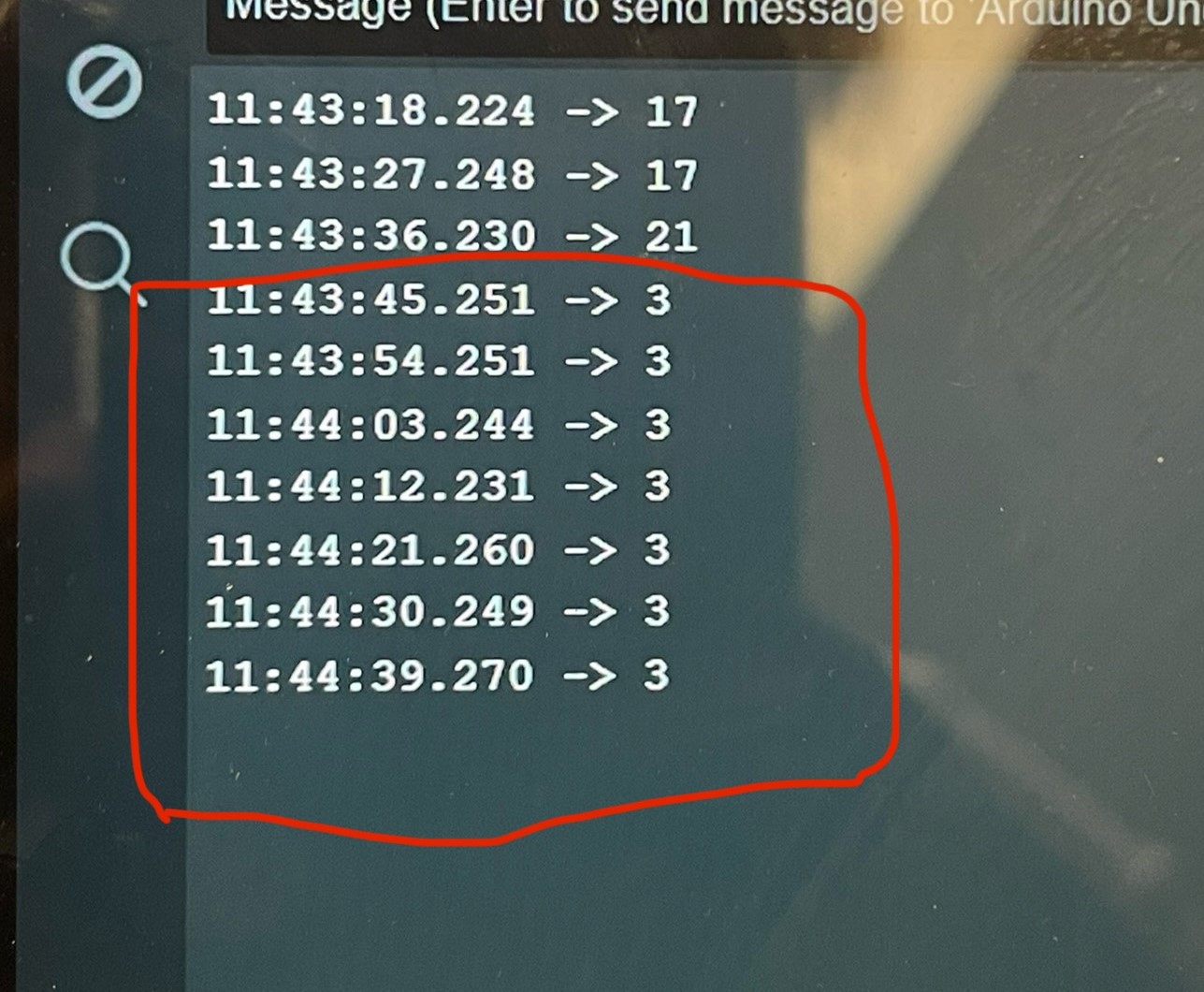
The Arduino code shown in Figure 3 is designed to communicate
with an SPI device. In the "setup()" function, it initializes the
serial communication at 9600 bps and configures pin 13 as an output,
pin 10 as an output for the chip select (CS) function, and pin 12 as an
input. It then sets the CS pin high and initializes the SPI bus. In the
main "loop()", it starts an SPI transaction with16 MHz clock speed, MSB
first and SPI mode 3. It pulls the CS pin low to enable the SPI device,
and transfers one byte of data, storing the received byte into
"receivedData10". After the transfer, it sets the CS pin high and ends
the SPI transaction. If "cnt" is 8, it prints the received byte to the
serial monitor and resets "cnt" to 0; otherwise, it increments "cnt".
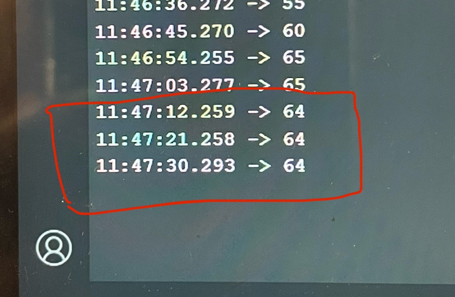
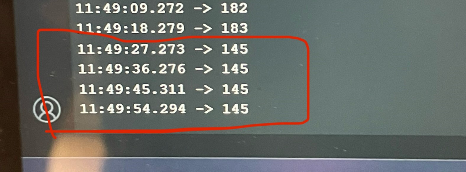
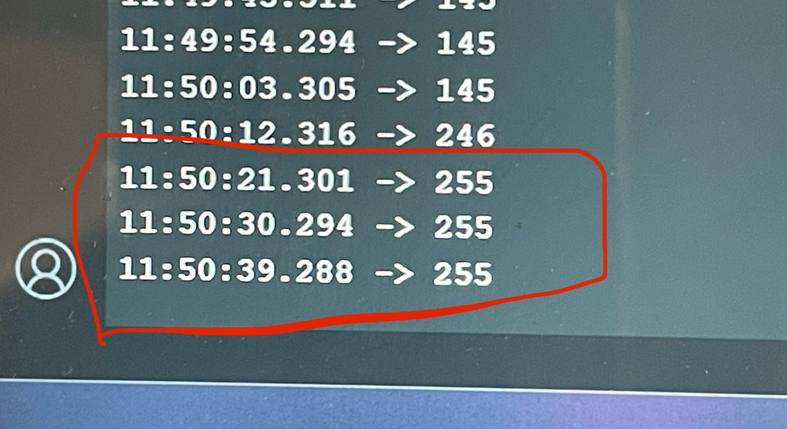
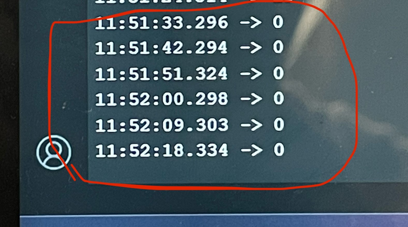
The loop runs every second due to the "delay(1000)". When we were
reading the data we realized that, there was a problem in the
synchronicity of the clocks and we were seeing the right value in every
eighth reads. So we made the SPI device the read and print the value
periodically in every eighth read.
Figure 3. Arduino SPI controller receiver code
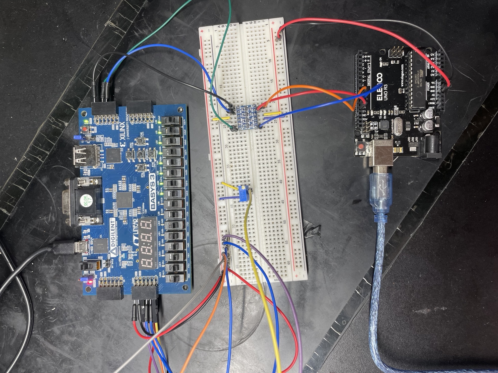
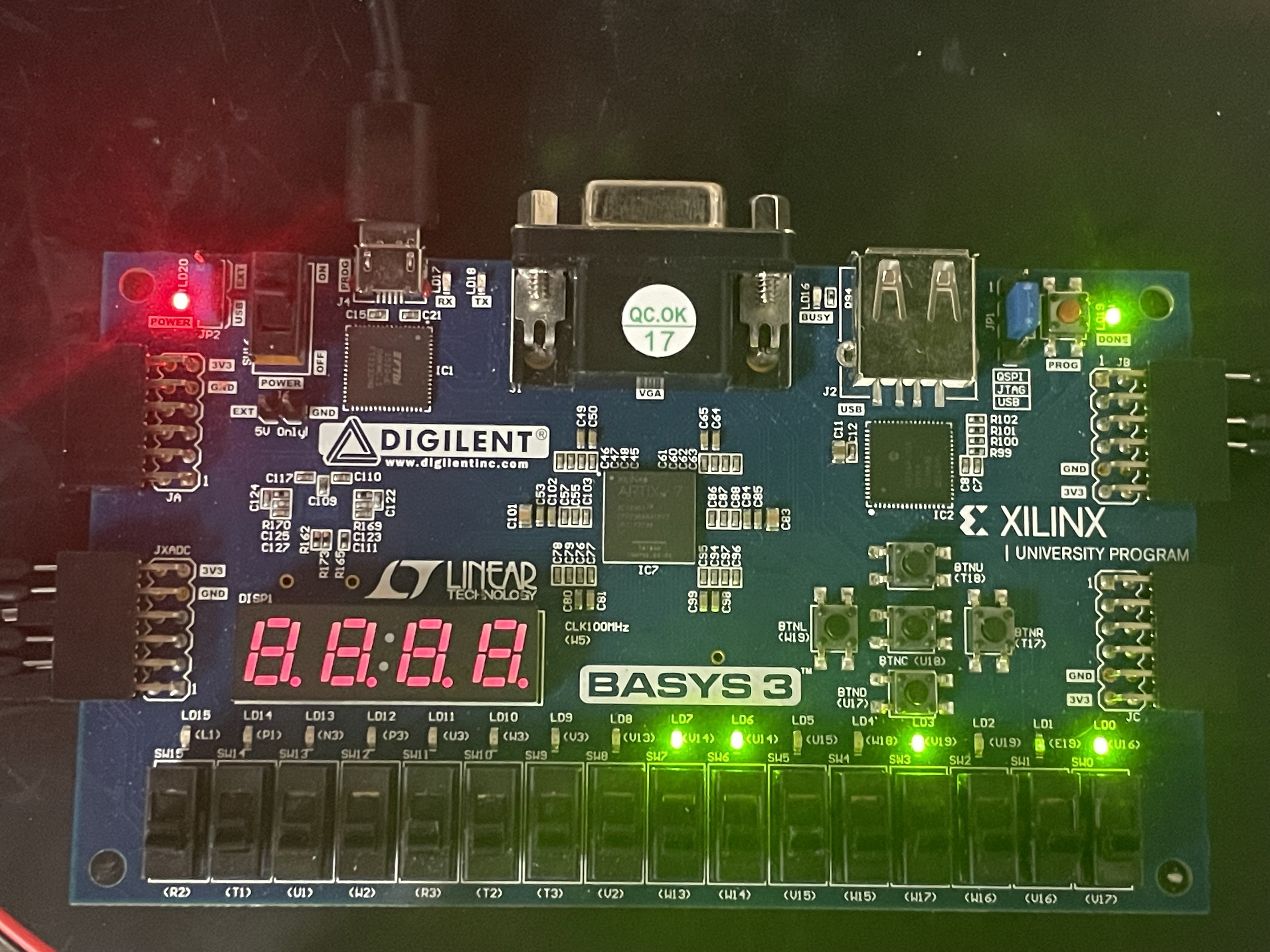
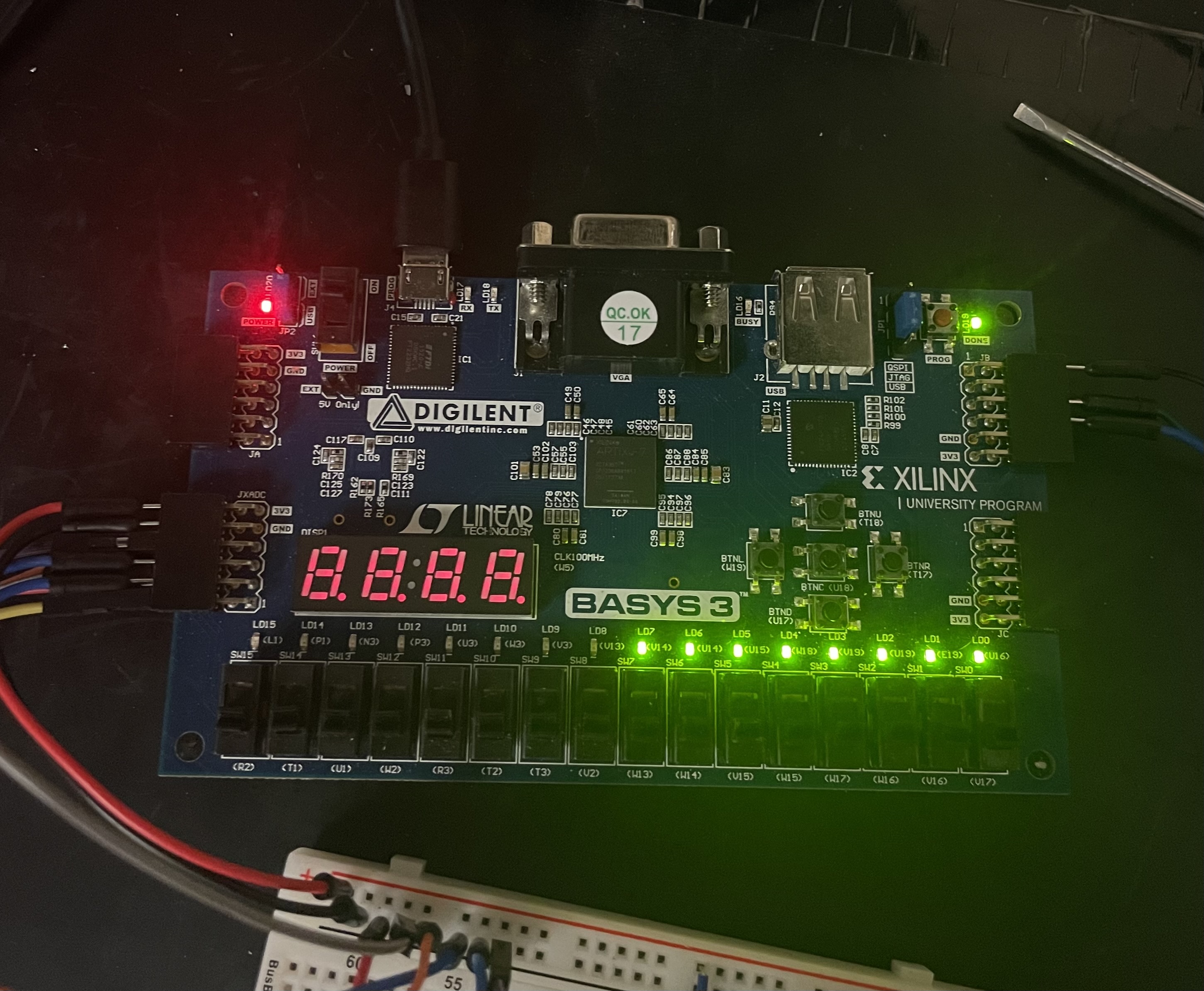
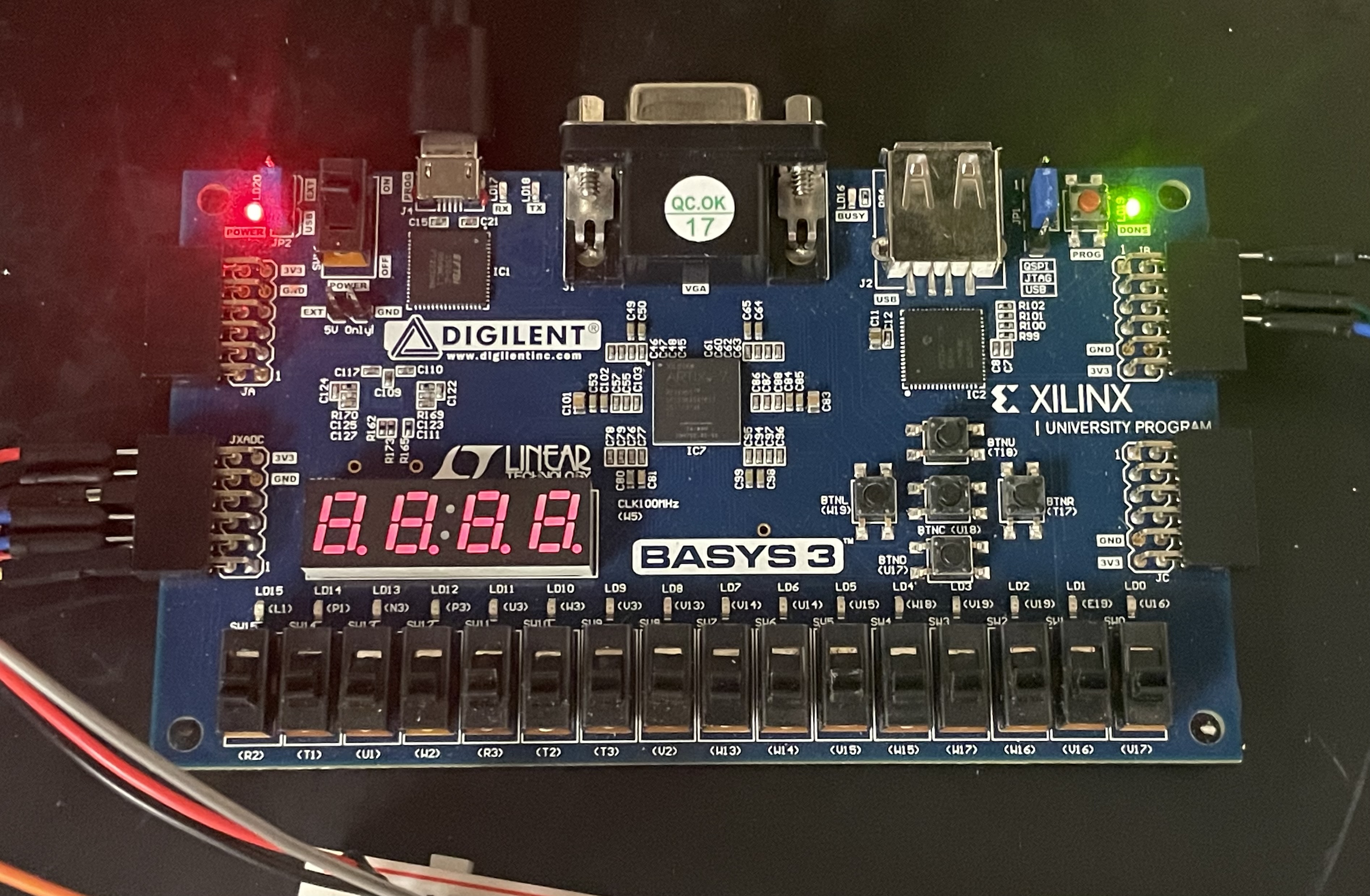
Figure 4. The setup of the FPGA, breadboard and arduino board
Video 1. The demonstration of ADC working on the serial monitor