Class Project:
Build a SAR ADC
By: Roxie Sandoval
rlsandoval@fortlewis.edu
I. Introduction
The purpose of this project was to build a working 8-bit Successive Approximation Register or SAR using Electric VSLI. A SAR ADC, converts a sampled voltage to digital output, hence ADC or Analog to Digital Converter. Since a working SAR uses multiple components they were each tested using LTSpice simulation.
II. Methods and Materials
III. Results
Figure 1 and 2 below show the sample and hold schematic and the results simulated in LTSpice. However, for unknown reasons the sampling rate is off, this could be due to the code or in the circuit.
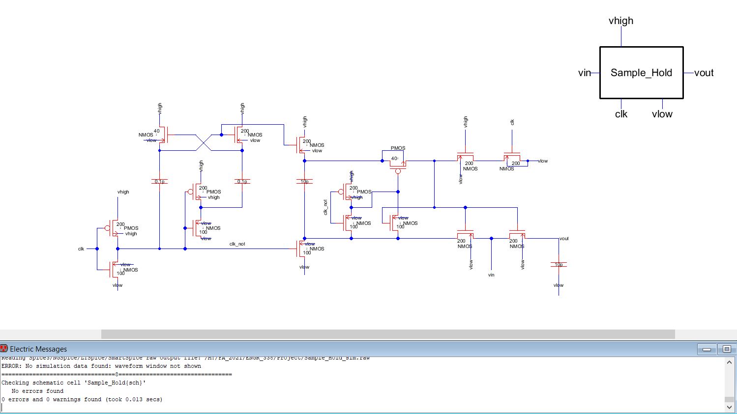
Figure 1: The schematic of the Sample and Hold, with the icon in the upper right corner.
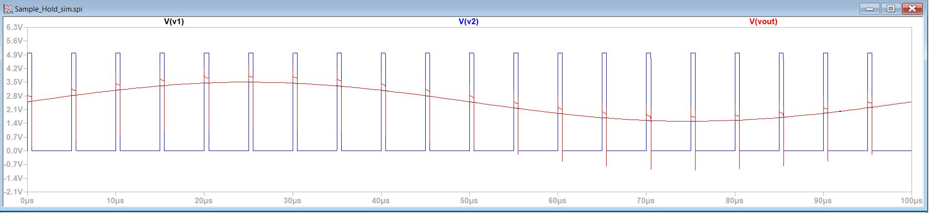
Figure 2: The results of the sample and hold simulated in LTSpice. There is an error in the cirsuit or code that the sampling is off.
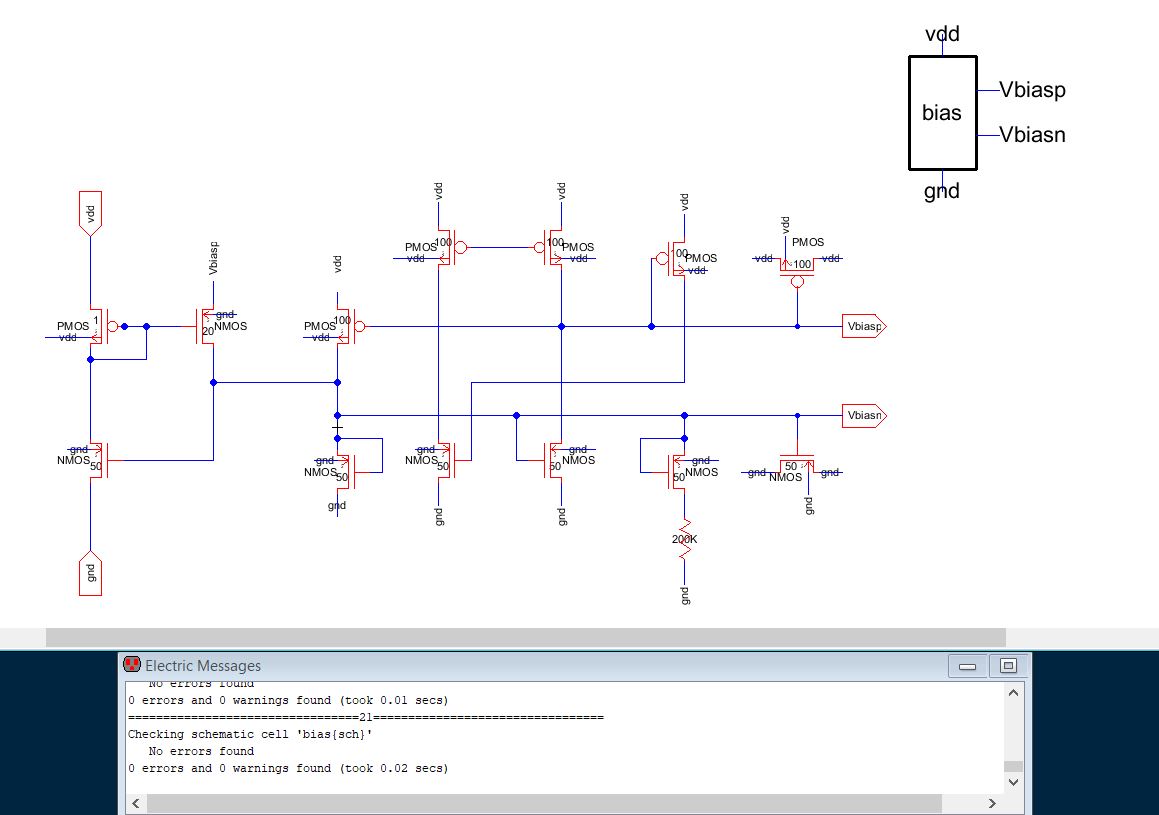
Figure 3: The biasing circuit used in the op-amp circuit.
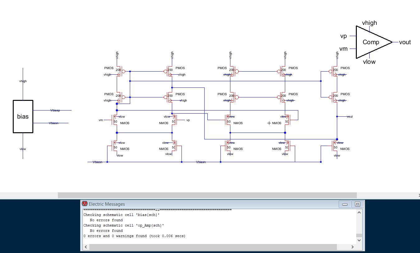
Figure 4: The op-amp schematic with the bias icon in the lower left corner and the op-amp icon in the right corner.

Figure 5: Using two inverters, the buffer was created that will be used in the SAR block circuit.
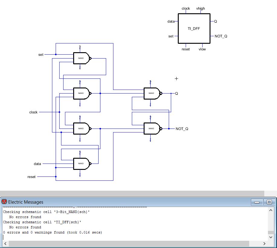
Figure 6: Using a 3-input NAND gates to create D-flip flops.
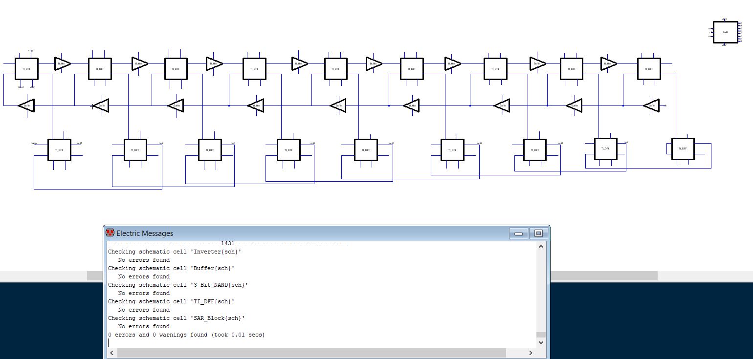
Figure 7: The SAR block with the buffers and D-Flip flops and clean of errors.
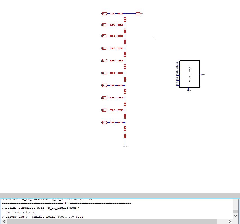
Figure 8: From a previous lab the R-2R ladder was used and checked for errors.
IV. Discussion
Due to some errors in circuit design and coding, I was unable to complete the project. Though I did learn from my mistakes, such as the orientation of the NMOS and PMOS, personally trying to translate between LTSpice and Electric created a learning curve.
The purpose of this project was to build a working 8-bit Successive Approximation Register or SAR using Electric VSLI. A SAR ADC, converts a sampled voltage to digital output, hence ADC or Analog to Digital Converter. Since a working SAR uses multiple components they were each tested using LTSpice simulation.
II. Methods and Materials
i. Materials
1. Electric VSLI
2. LTSpice Software
ii. Methods
First, the schematic for the sample and hold component was created in Electric, it was then tested for error and finally simulated. The same would be done for the operational amplifier, biasing circuit, SAR block, and R-2R ladder.
1. Electric VSLI
2. LTSpice Software
ii. Methods
First, the schematic for the sample and hold component was created in Electric, it was then tested for error and finally simulated. The same would be done for the operational amplifier, biasing circuit, SAR block, and R-2R ladder.
III. Results
Figure 1 and 2 below show the sample and hold schematic and the results simulated in LTSpice. However, for unknown reasons the sampling rate is off, this could be due to the code or in the circuit.
Figure 1: The schematic of the Sample and Hold, with the icon in the upper right corner.
Figure 2: The results of the sample and hold simulated in LTSpice. There is an error in the cirsuit or code that the sampling is off.
Figure 3 below is the biasing schematic that will be used in the op-amp.
Figure 3: The biasing circuit used in the op-amp circuit.
The op-amp or operational amplifier schematic can be seen below in Figure 4.
Figure 4: The op-amp schematic with the bias icon in the lower left corner and the op-amp icon in the right corner.
In Figure 5 below, the buffer's schematic and icon can be seen, which uses two inverters from a previous lab.
Figure 5: Using two inverters, the buffer was created that will be used in the SAR block circuit.
Using a 3-input NAND gates to create a D-Flip Flop as seen in Figure 6, below. The D-Flip Flop will be used in the SAR circuit.
Figure 6: Using a 3-input NAND gates to create D-flip flops.
The buffer and flip-flop are both used to creat the SAR block as seen in Figure 7.
Figure 7: The SAR block with the buffers and D-Flip flops and clean of errors.
From a previous lab, the R-2R ladder schematic as seen in Figure 8, as well as the icon to the right.
Figure 8: From a previous lab the R-2R ladder was used and checked for errors.
IV. Discussion
Due to some errors in circuit design and coding, I was unable to complete the project. Though I did learn from my mistakes, such as the orientation of the NMOS and PMOS, personally trying to translate between LTSpice and Electric created a learning curve.