Lab 9:
Design an 8-Bit ALU
By: Roxie Sandoval
rlsandoval@fortlewis.edu
I. Introduction
The objective of this lab was to build an 8-bit ALU. An ALU or an arithmetric logic unit can perform AND, OR, ADDITION, and SUBTRACTIONS operations.
II. Materials
III. Results
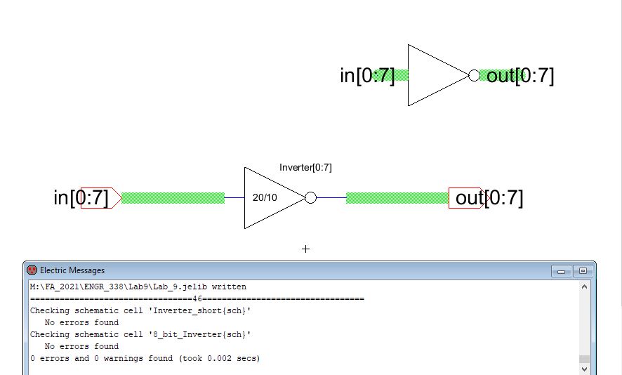
Figure 1: The schematic of the 8-bit schematic with zero errors.
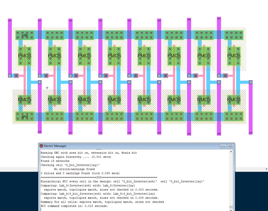
Figure 2: The layout of the 8-bit inverter with the matching topologies and no errors.
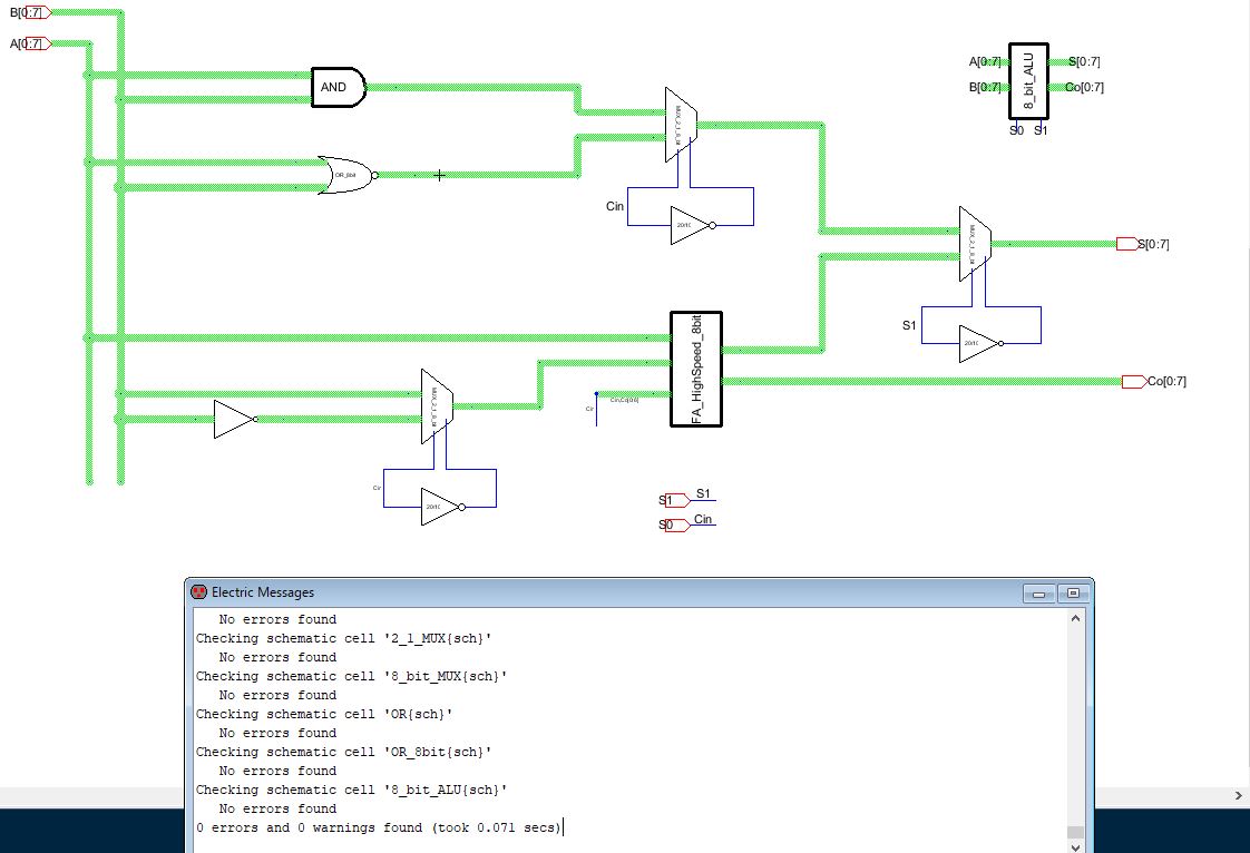
Figure 3: The 8-bit ALU schematic with no errors.
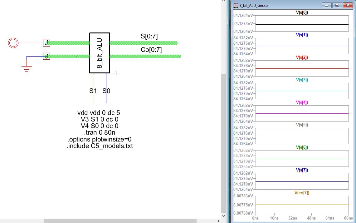
Figure 4: The ALU icon was used to verify the AND logic, results can be seen on the right.
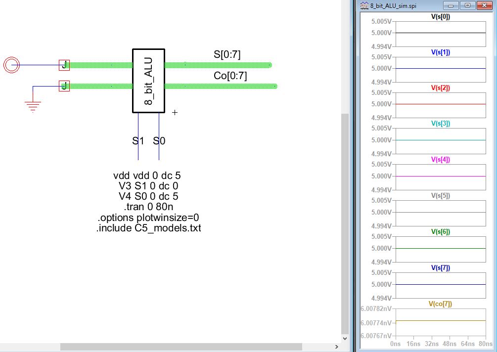
Figure 5: The OR logic was verified using the schematic, the results can be seen on the right.
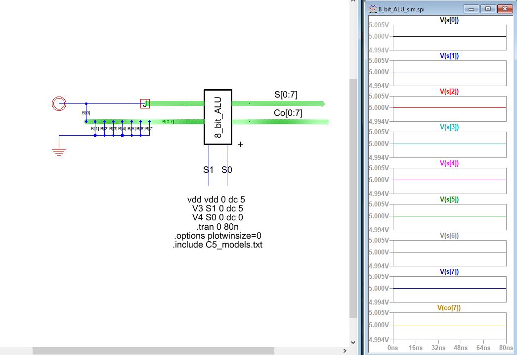
Figure 6: The ADD operation was also verified, again the results on the right.
Figure 6: Last operation, SUBTRACTION was verified, results are shown on the right.

Figure 7: The 8-bit ALU layout, with zero errors and matching topologies.
IV. Discussion
Overall the lab can be considered a success, because it increased my understanding and showed how the ALU performs, by testing the logic and designing the layout.
The objective of this lab was to build an 8-bit ALU. An ALU or an arithmetric logic unit can perform AND, OR, ADDITION, and SUBTRACTIONS operations.
II. Materials
i. Materials
1. ElectricVLSI software
2. LTSpice software
2. LTSpice software
ii. Methods
Similiar
to previous labs, the 8-bit schematic of the ALU was
created first, however since an 8-bit inverter was needed, both the
schematic and the layout were built. When the inverter was tested to
show zero errors and the topologies matched, and the logic was verified
using LTSpice, it was used in the final 8-bit ALU design.
Once, the 8-bit ALU schematic was created, it was then converted to an icon, which was used to test the logic and operations with LTSpice. After verification, the layout was designed and checked for errors and matching topologies.
Once, the 8-bit ALU schematic was created, it was then converted to an icon, which was used to test the logic and operations with LTSpice. After verification, the layout was designed and checked for errors and matching topologies.
III. Results
i. The 8-bit Inverter
Figure 1, shows the schematic for the 8-bit inverter, with no errors and in the upper right corner the icon can be seen, which was used to verify the logic, as seen in Figure 2.
Figure 1, shows the schematic for the 8-bit inverter, with no errors and in the upper right corner the icon can be seen, which was used to verify the logic, as seen in Figure 2.
Figure 1: The schematic of the 8-bit schematic with zero errors.
Figure 2: The layout of the 8-bit inverter with the matching topologies and no errors.
ii. The 8-bit ALU
Figure 3, shows the 8-bit ALU schematic with zero errors. Again, the ison can be seen in the upper right corner which was used to verify the logic and operations. Figure 4, shows the ALU icon schematic, used to verify the AND logic.
Figure 3, shows the 8-bit ALU schematic with zero errors. Again, the ison can be seen in the upper right corner which was used to verify the logic and operations. Figure 4, shows the ALU icon schematic, used to verify the AND logic.
Figure 3: The 8-bit ALU schematic with no errors.
Figure 4: The ALU icon was used to verify the AND logic, results can be seen on the right.
The
OR logic and both the addition and subtraction operations were all
verified using the ALU icon, each of the schematics and results can be
seen in Figures 4,5 and 6, below.
Figure 5: The OR logic was verified using the schematic, the results can be seen on the right.
Figure 6: The ADD operation was also verified, again the results on the right.
Figure 6: Last operation, SUBTRACTION was verified, results are shown on the right.
Lastly,
the layout of the 8-bit ALU can be seen below in Figure 7.
Because each of the components were from previous labs, it was
important that there were no errors.
Figure 7: The 8-bit ALU layout, with zero errors and matching topologies.
IV. Discussion
Overall the lab can be considered a success, because it increased my understanding and showed how the ALU performs, by testing the logic and designing the layout.