Lab 8:
Design a MUX, and a Hgh Speed Full Adder
By: Roxie Sandoval
rlsandoval@fortlewis.edu
I. Introduction
The objectives of this lab were to build a MUX and a high speed full adder in ElectricVLSI and simulated in LTSpice.
II. Materials
i. Materials
1. ElectricVLSI software
2. LTSpice software
2. LTSpice software
ii. Methods
The schematic for a MUX was designed and simulated in LTSpice for verification of the logic. Once the logic was verified and the schematic was clear of errors, a layout of the MUX was created, checked for errors and matching hierarchy. The mux icon and layout were used to create an 8-bit MUX, this too was simulated, checked for errors and matching topographies. Next, the schematic and icon for a full speed adder was created, checked and simulated to verify the logic. Then the layout of the full adder was built, checked again. Lastly, the 8-bit high speed full adder schematic was created and tested, then the layout was built, checked for errors and matching topographies.
The schematic for a MUX was designed and simulated in LTSpice for verification of the logic. Once the logic was verified and the schematic was clear of errors, a layout of the MUX was created, checked for errors and matching hierarchy. The mux icon and layout were used to create an 8-bit MUX, this too was simulated, checked for errors and matching topographies. Next, the schematic and icon for a full speed adder was created, checked and simulated to verify the logic. Then the layout of the full adder was built, checked again. Lastly, the 8-bit high speed full adder schematic was created and tested, then the layout was built, checked for errors and matching topographies.
III. Results
i. Mux
Shown in Figure 1, below shows 1-bit MUX with the spice code, that would be used in the simulation to prove the logic, which can be seen on the right. After verfication, the layout can be seen in Figure 2.
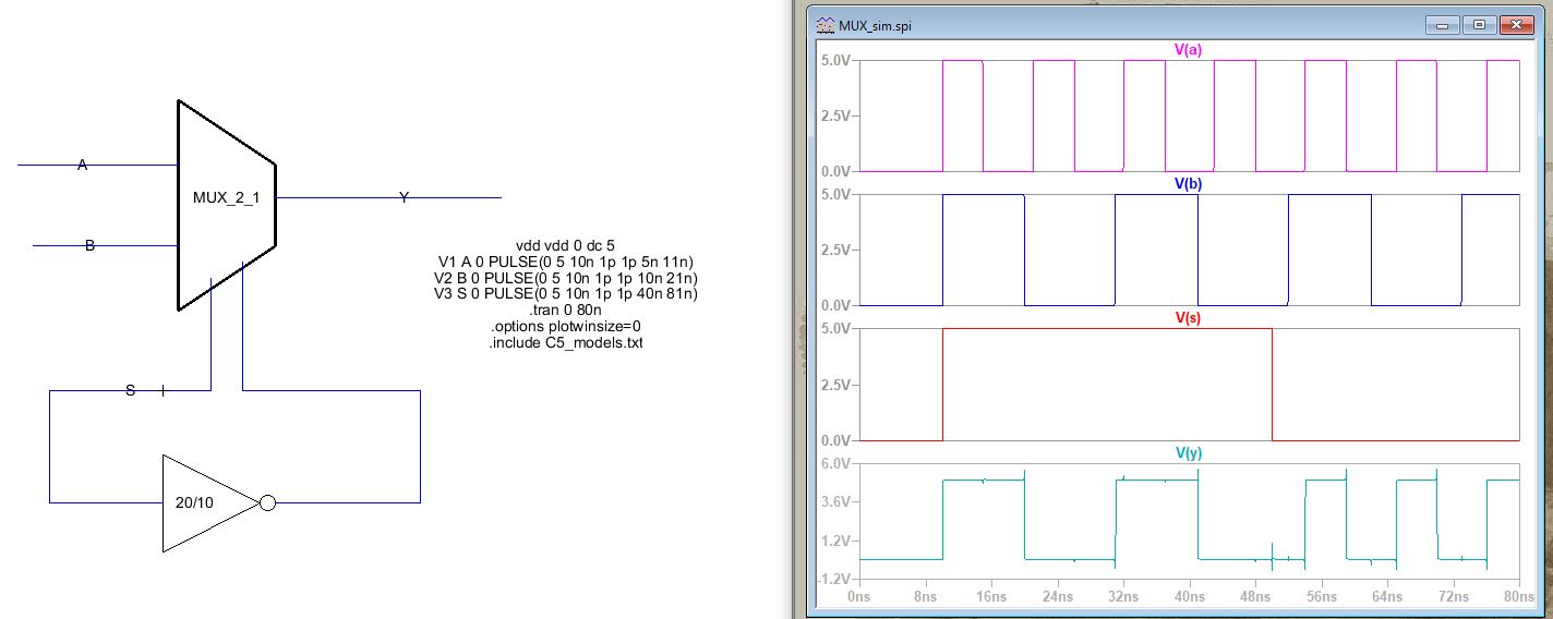
Figure 1: The 8-bit MUX simulation and LTSpice results.
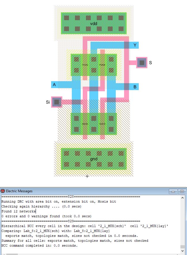
Figure 2: The layout of the MUX, with clean errors and matching topologies.
Shown in Figure 1, below shows 1-bit MUX with the spice code, that would be used in the simulation to prove the logic, which can be seen on the right. After verfication, the layout can be seen in Figure 2.
Figure 1: The 8-bit MUX simulation and LTSpice results.
Figure 2: The layout of the MUX, with clean errors and matching topologies.
ii. 8-bit MUX
Without using buses, a longer and more tedious schematic can be seen in Figure 3, and using buses shows a more compact schematic as shown in Figure 4. Using the schematic in Figure 4, it was used in a simulation to verify the logic, as well. Then the 8-bit layout was created and tested.
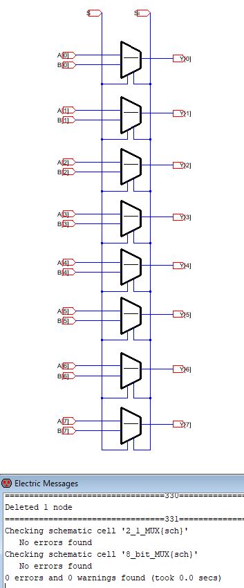
Figure 3: A full schematic of the 8-bit MUX.
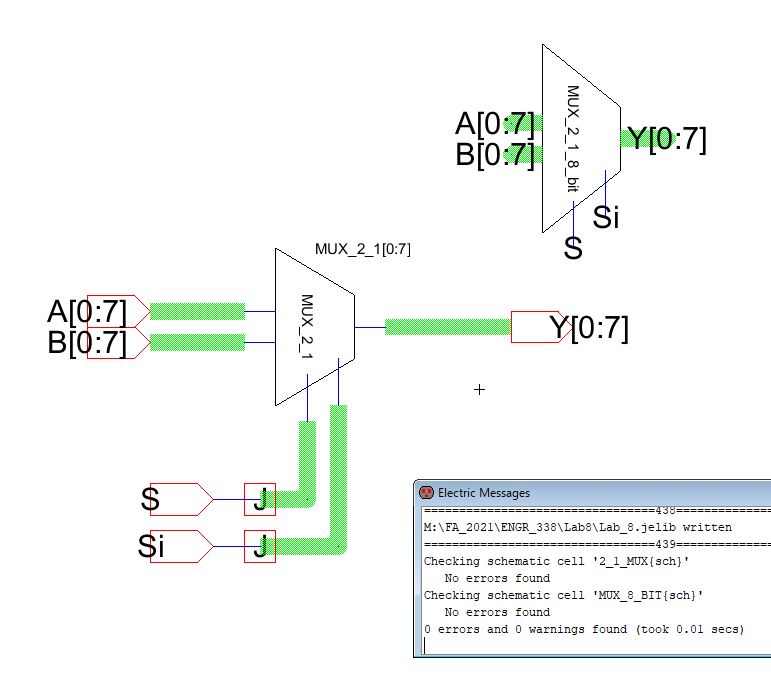
Figure 4: The schematic of the 8-bit MUX using buses and the icon in the upper right corner.
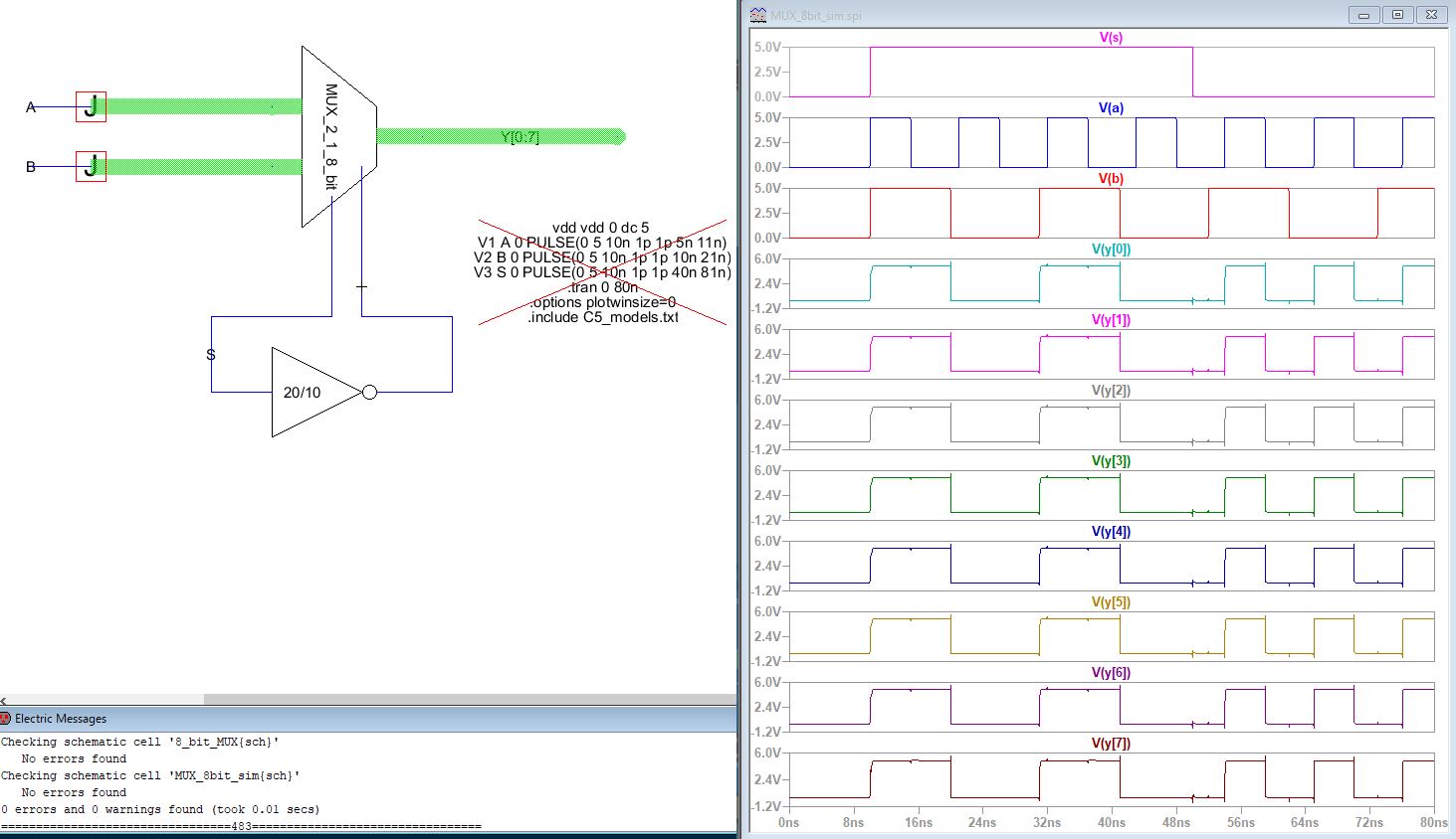
Figure 5: The simulation of the 8-bit MUX and the results on the right.
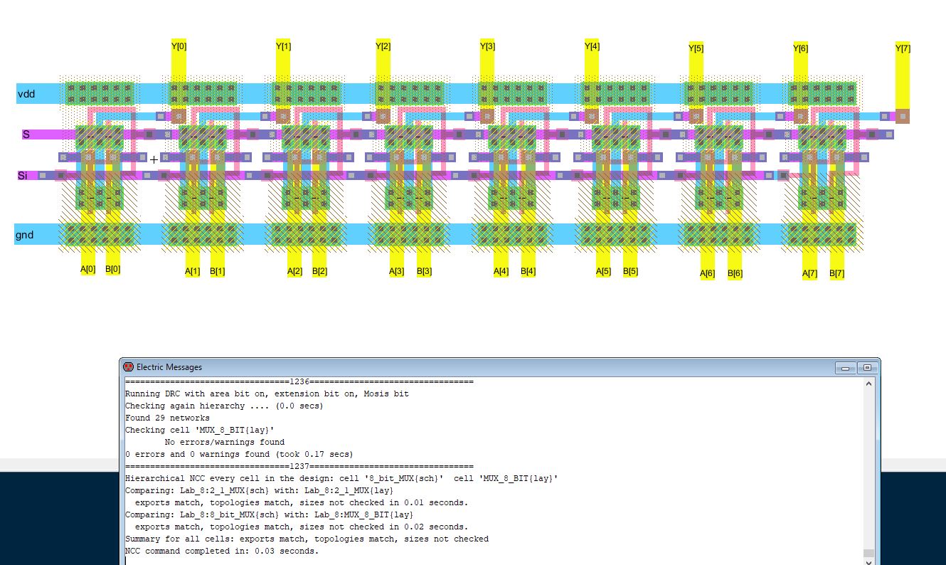
Figure 6: The layout of the 8-bit MUX free of errors and matching topologies.
IV. Discussion
The lab is considered a success, since the resulting 8-bit MUX and full adder both had clean DRCs and matching topograghies. Although both were very tedious in creating, because connecting the wires was difficult and had to be sure they were connected to the correct ports.
Without using buses, a longer and more tedious schematic can be seen in Figure 3, and using buses shows a more compact schematic as shown in Figure 4. Using the schematic in Figure 4, it was used in a simulation to verify the logic, as well. Then the 8-bit layout was created and tested.
Figure 3: A full schematic of the 8-bit MUX.
Figure 4: The schematic of the 8-bit MUX using buses and the icon in the upper right corner.
Figure 5: The simulation of the 8-bit MUX and the results on the right.
Figure 6: The layout of the 8-bit MUX free of errors and matching topologies.
iii. High Speed Full Adder
In Figure 7, the schematic of the high speed full adder can be seen, to be sure there were no issues later in construction, this had to have zero errors. The logic also had to be verified as seen in Figure 8, once the full adder was responding as expected, the layout was built, Figure 9. This layout will be used in the 8-bit full adder, it had to be checked for errors and matching topologies.
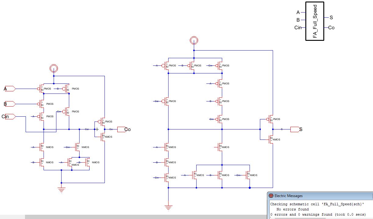
Figure 7: Schematic of the high speed full adder, with clean DRC.
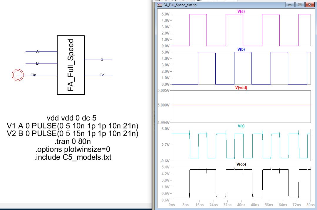
Figure 8: The simulation and results of the full speed full adder.
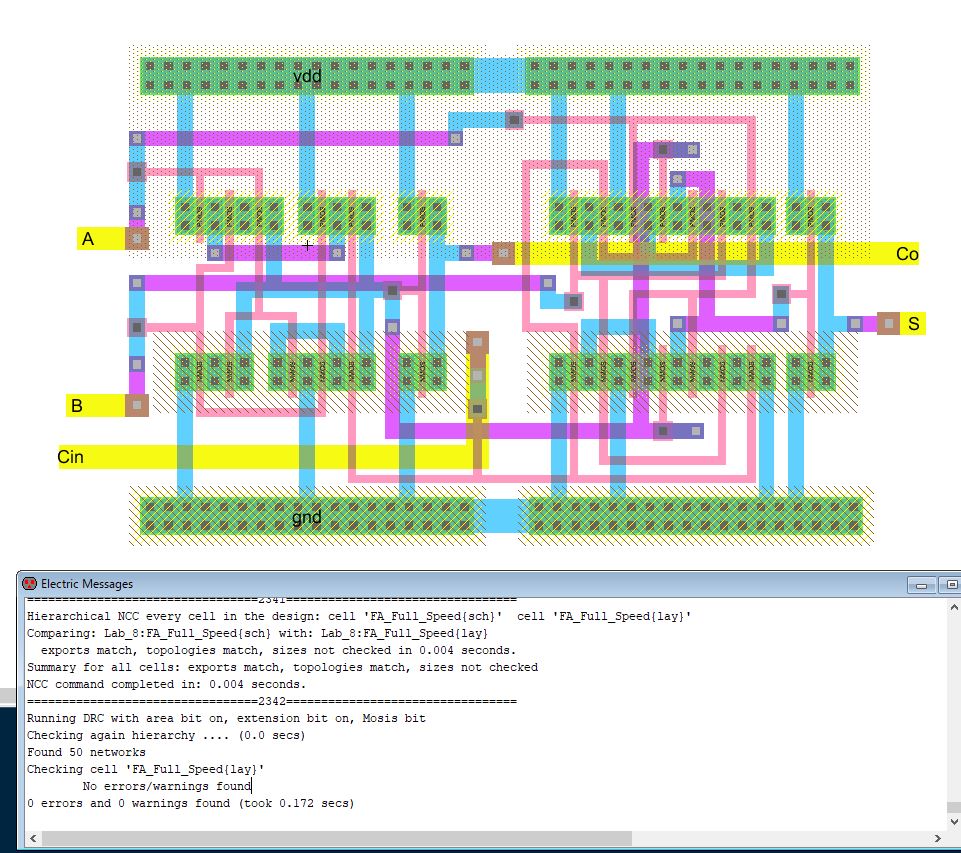
Figure 9: The High speed full adder layout with zero errors and matching hierarchy.
In Figure 7, the schematic of the high speed full adder can be seen, to be sure there were no issues later in construction, this had to have zero errors. The logic also had to be verified as seen in Figure 8, once the full adder was responding as expected, the layout was built, Figure 9. This layout will be used in the 8-bit full adder, it had to be checked for errors and matching topologies.
Figure 7: Schematic of the high speed full adder, with clean DRC.
Figure 8: The simulation and results of the full speed full adder.
Figure 9: The High speed full adder layout with zero errors and matching hierarchy.
i. 8-bit High Speed Full Adder
Once, the 1-bit full adder had a clean DRC and NCC, the schematic was created as seen below in Figure 10. This was simulated in LTSpice, as well, shown in Figure 11. Lastly, the layout was created and can be seen in Figure 12, with the clean error and matching topologies message.
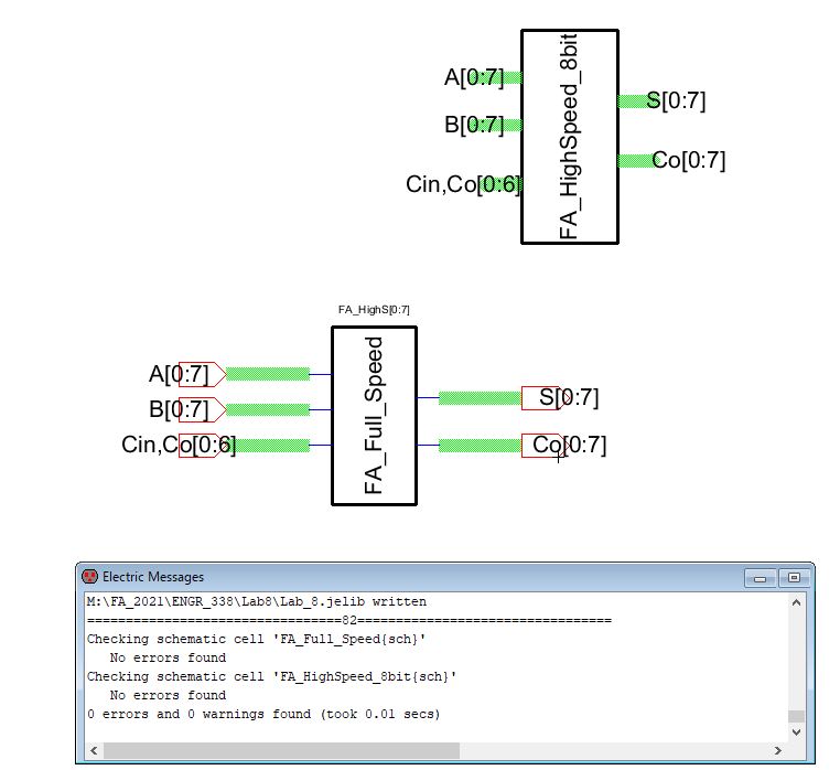
Figure 10: A schematic of the 8-bit full adder using buses.
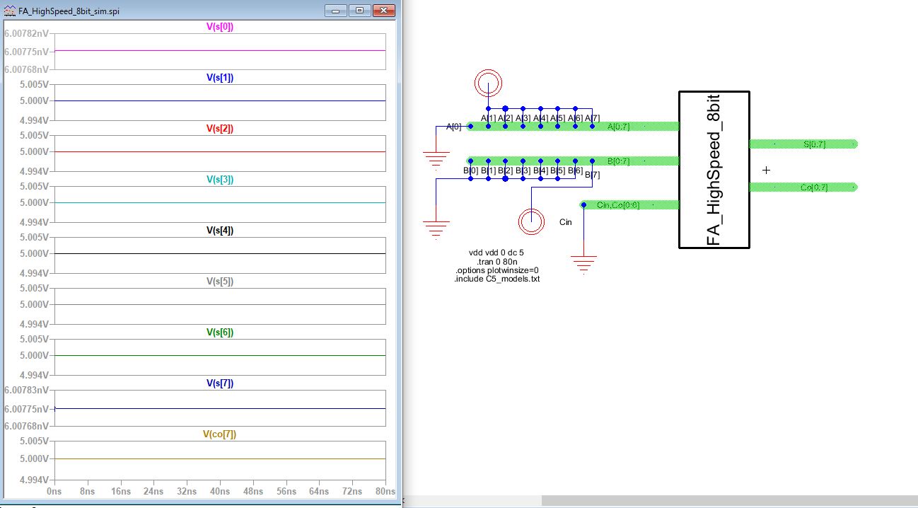
Figure 11: The simulation for the 8-bit full adder and results on the left.
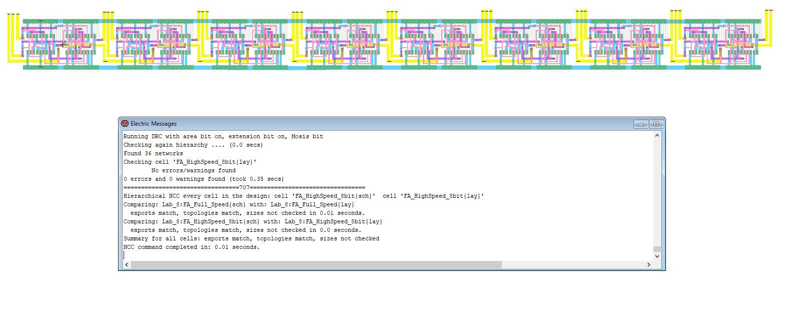
Figure 12: A 8-bit full adder layout, with no errors and matching topographies.
Once, the 1-bit full adder had a clean DRC and NCC, the schematic was created as seen below in Figure 10. This was simulated in LTSpice, as well, shown in Figure 11. Lastly, the layout was created and can be seen in Figure 12, with the clean error and matching topologies message.
Figure 10: A schematic of the 8-bit full adder using buses.
Figure 11: The simulation for the 8-bit full adder and results on the left.
Figure 12: A 8-bit full adder layout, with no errors and matching topographies.
IV. Discussion
The lab is considered a success, since the resulting 8-bit MUX and full adder both had clean DRCs and matching topograghies. Although both were very tedious in creating, because connecting the wires was difficult and had to be sure they were connected to the correct ports.