Lab 7:
Using Buses in ElectricVLSi
By: Roxie Sandoval
rlsandoval@fortlewis.edu
I. Introduction
The objectives of this lab were to build a ring oscillator using buses and multi-bit gates in ElectricVLSI and simulated in LTSpice.
II. Materials
III. Results
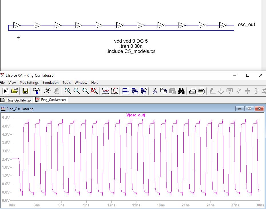
Figure 1: First simulation of the ring oscillator uses 11 inverters.
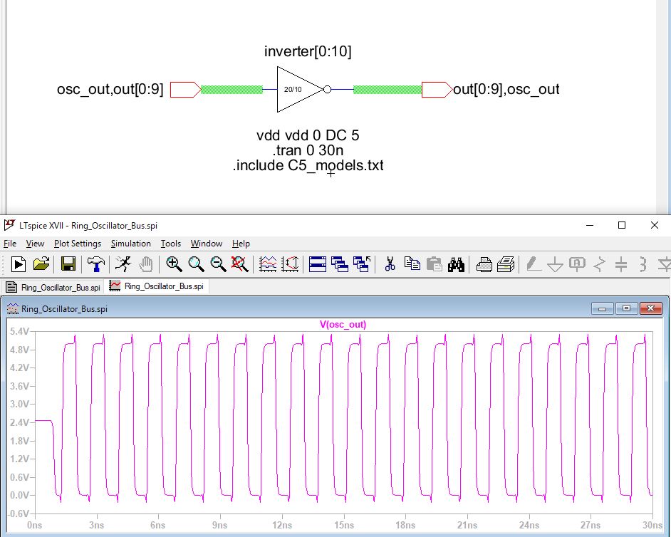
Figure 2: Second simulation of the ring oscillator uses the bus (green wires) instead of 11 inverters.
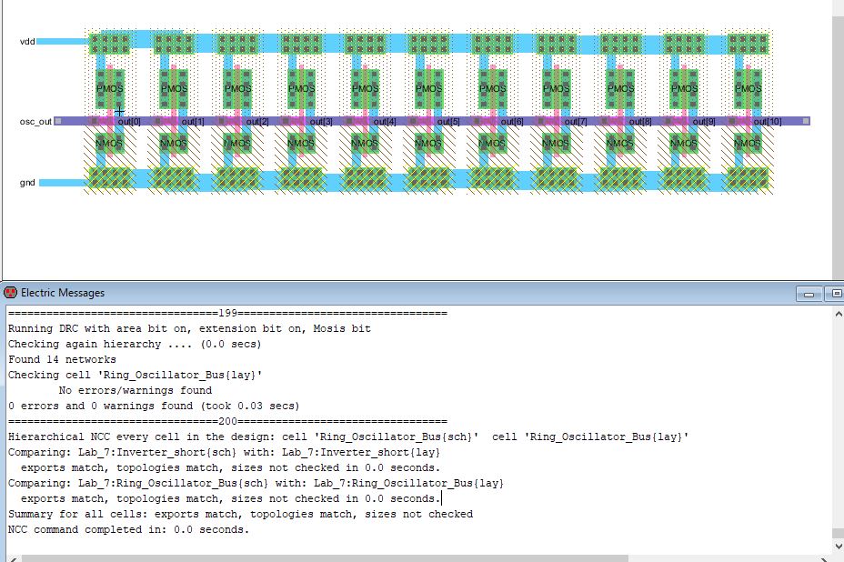
Figure 3: The ring oscillator layout with matching topologies and zero errors.
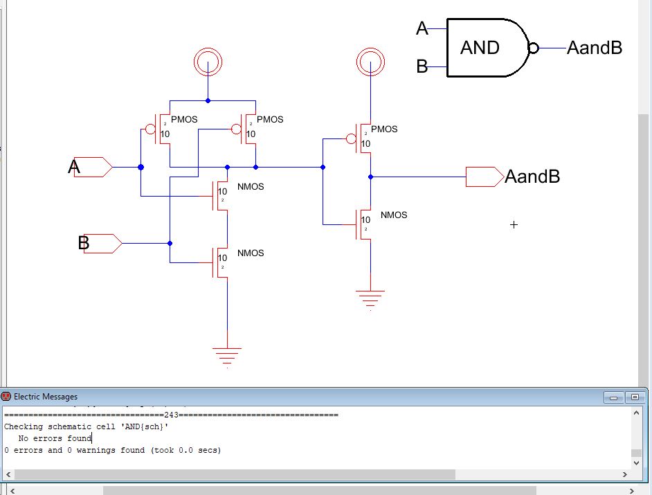
Figure 4: The AND logic schematic with zero errors, and icon in the upper right corner.
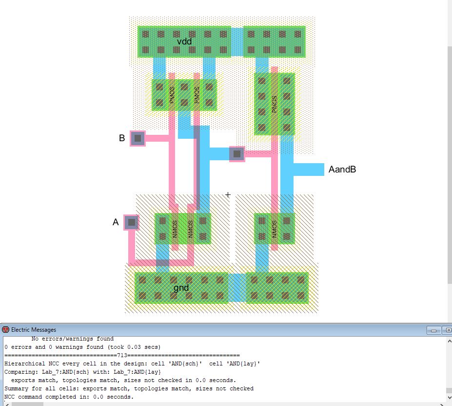
Figure 5: The AND logic gate layout with matching topologies and zero errors.
To test the AND logic, it was simulated twice using LTSpice, Figure 6 displays the first schematic and simulation results, here the A-port is connected to a voltage source. In Figure 7, the A-port is shorted to ground, the results can also be seen below the schematic.
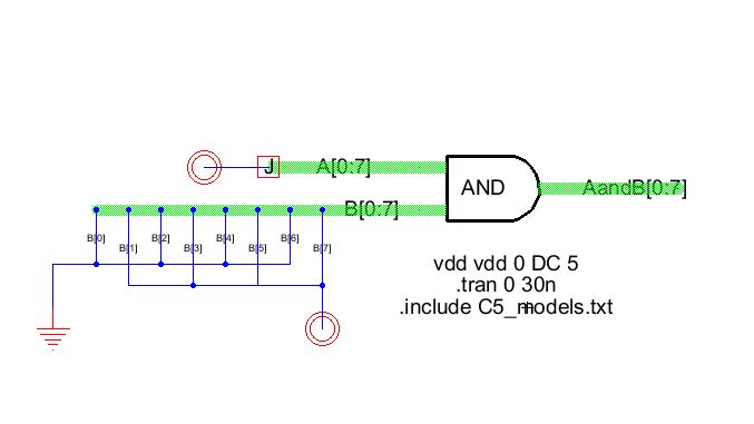

Figure 6: The first 8-bit schematic using the AND gate icon for simulation and results.
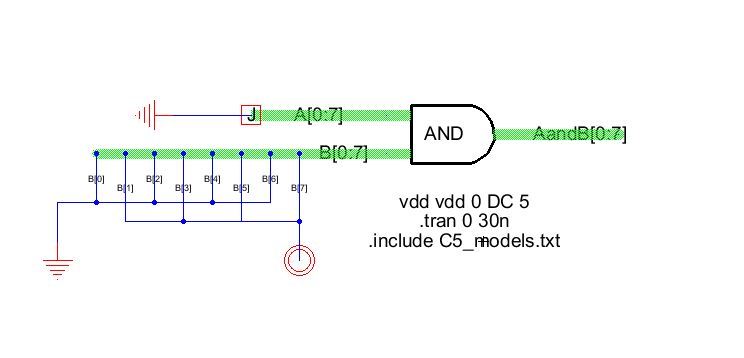
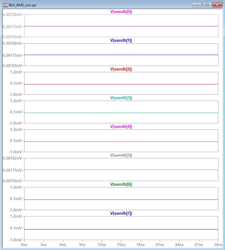
Figure 7: The second 8-bit schematic using the AND gate icon for simulation and results.
Because the simulations were correct, the 8-bit AND gate layout was created and tested for errors and the topology was analyzed to ensure it matched the previous schematics, seen below in Figure 8.
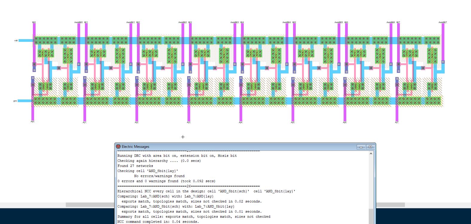
Figure 8: The 8-bit AND gate layout with zero errors and matching topologies.
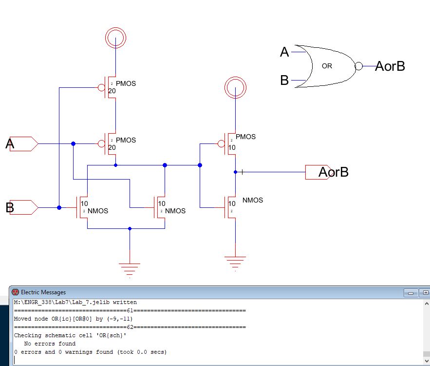
Figure 9: The OR schematic with the icon in the upper right corner.
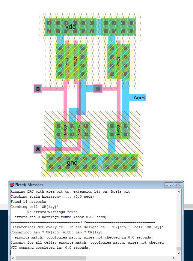
Figure 10: The layout for the the OR gate with zero errors.
Figure 11 show the simulation for the OR gate, this was to check the logic, before creating the 8-bit logic gate.
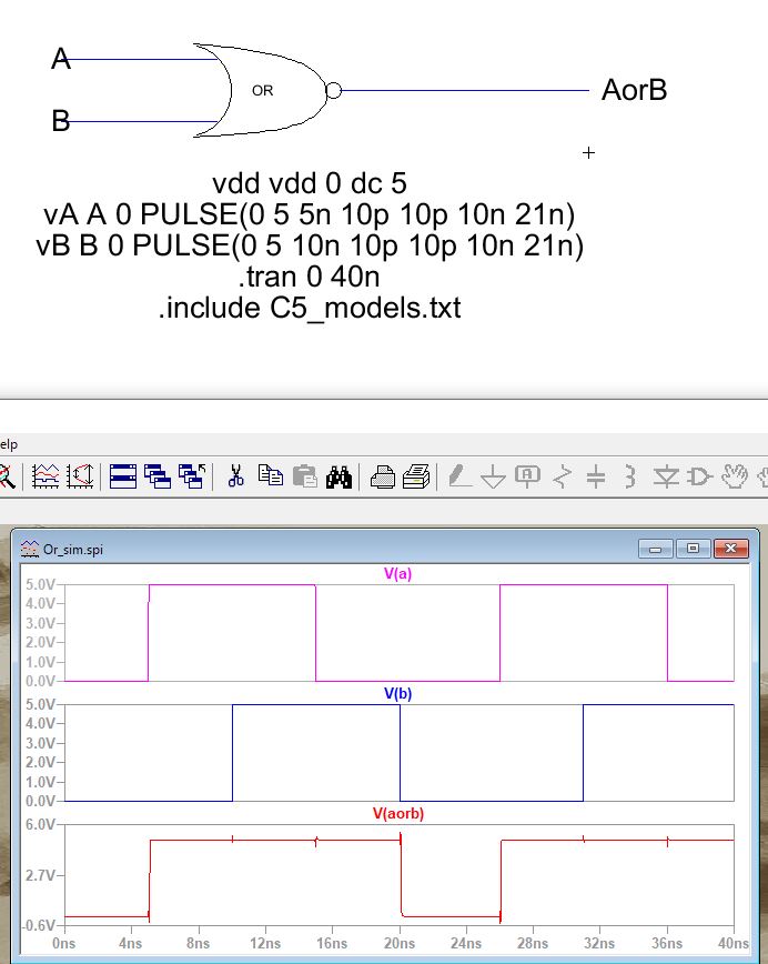
Figure 11: A schematic and results for the OR gate.
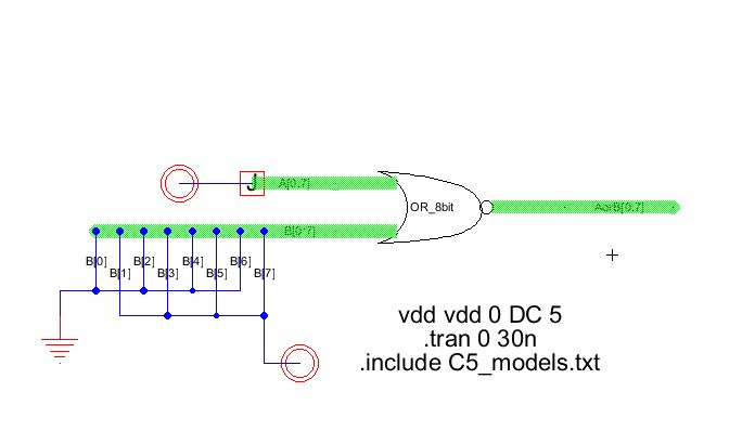
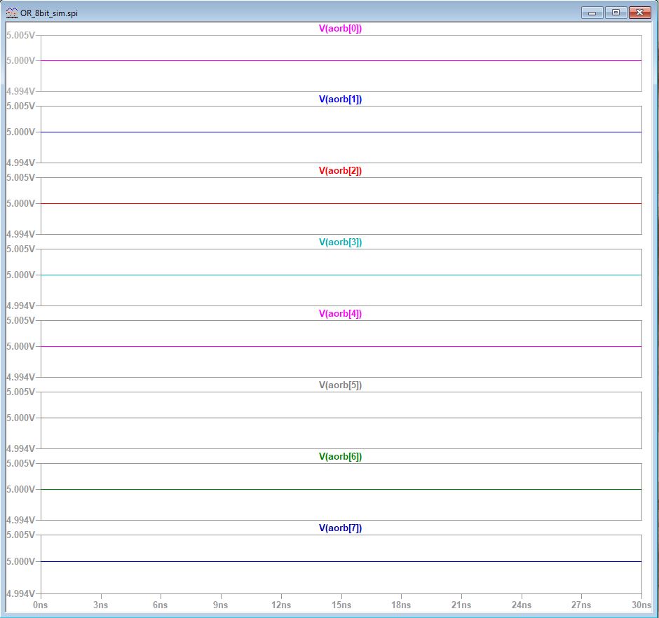
Figure 12: The schematic and results for the 8-bit OR gate.
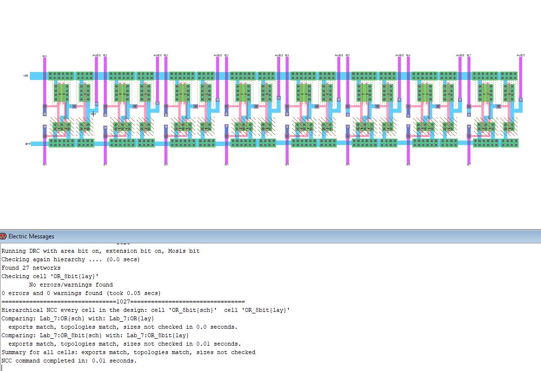
Figure 13: The OR gate layout with matching topologies and zero errors.
iv. 8-bit NAND gate
Since the NAND gate was built in a previous lab, Figure 14 shows the 8-bit simulation and results obtained from the LTSpice.
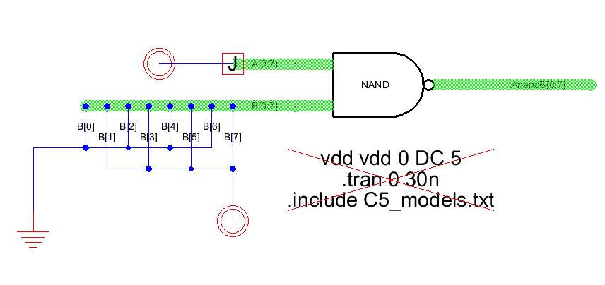
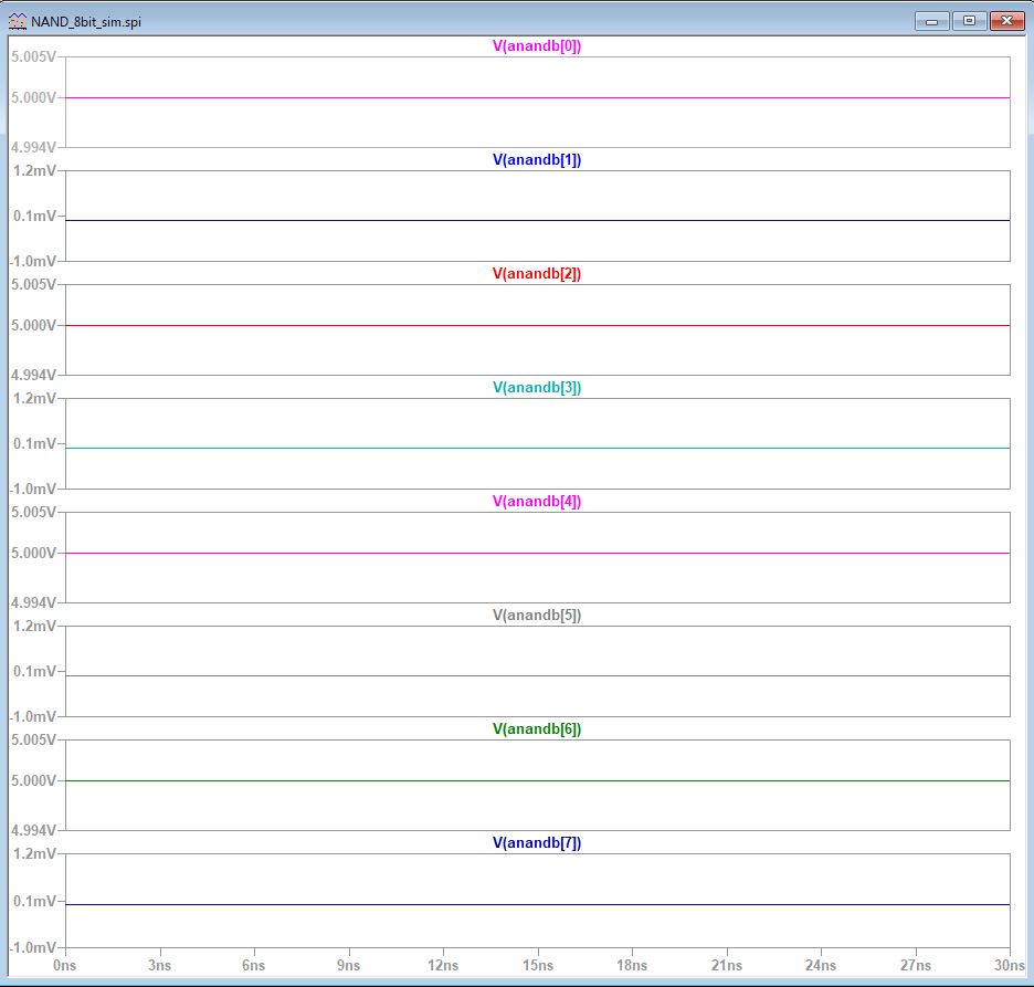
Figure 14: The schematic and results for the 8-bit NAND gate.
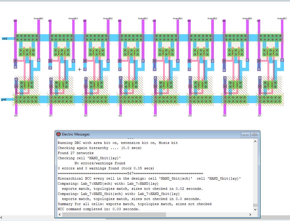
Figure 15: The 8-bit NAND gate layout with zero errors and matching topologies.
IV. Discussion
The objective of the lab was to use buses to create a ring oscillator and multi-bit logic gates. This lab though tedious, can be considered to be a success since the objective was fullfilled, the bus showed how much easier it is to simulate a multi-bit gate. Although a bus could not be used in the layout for each of the components, because each of the ports cannot be connected to each other.
The objectives of this lab were to build a ring oscillator using buses and multi-bit gates in ElectricVLSI and simulated in LTSpice.
II. Materials
i. Materials
1. ElectricVLSI software
2. LTSpice software
ii. Methods
Some layouts and schematics for this lab used components from previous labs. The oscillator ring was created first, using the inverter from a previous lab. The schematic and layout were tested using LTSpice. Then a 8-bit AND, OR, NAND, and NOR gates were built, using layouts and schematic from previous labs, they were also NCC test to ensure the topologies match. The 8-bit logic gates were also simulated in LTSpice to check the logic.
III. Results
i. Oscillator ring
In Figure 1, the oscillator ring was first built using 11 inverters in series, the result is shown below the schematic. However, as seen in Figure 2, the results are the same as Figure 1 results, this is because the second simulation uses buses or the green wires.
In Figure 1, the oscillator ring was first built using 11 inverters in series, the result is shown below the schematic. However, as seen in Figure 2, the results are the same as Figure 1 results, this is because the second simulation uses buses or the green wires.
Figure 1: First simulation of the ring oscillator uses 11 inverters.
Figure 2: Second simulation of the ring oscillator uses the bus (green wires) instead of 11 inverters.
Figure 3 shows the layout for the oscillator ring using inverters from a previous lab.
Figure 3: The ring oscillator layout with matching topologies and zero errors.
ii. 8-bit AND Gate
Figure 4 and Figure 5 display the AND gate schematic and layout, respectively, both show zero errors - which is helpful when building the 8-bit AND gate.
Figure 4 and Figure 5 display the AND gate schematic and layout, respectively, both show zero errors - which is helpful when building the 8-bit AND gate.
Figure 4: The AND logic schematic with zero errors, and icon in the upper right corner.
Figure 5: The AND logic gate layout with matching topologies and zero errors.
To test the AND logic, it was simulated twice using LTSpice, Figure 6 displays the first schematic and simulation results, here the A-port is connected to a voltage source. In Figure 7, the A-port is shorted to ground, the results can also be seen below the schematic.
Figure 6: The first 8-bit schematic using the AND gate icon for simulation and results.
Figure 7: The second 8-bit schematic using the AND gate icon for simulation and results.
Because the simulations were correct, the 8-bit AND gate layout was created and tested for errors and the topology was analyzed to ensure it matched the previous schematics, seen below in Figure 8.
Figure 8: The 8-bit AND gate layout with zero errors and matching topologies.
iii. 8-bit OR gate
Similar to the AND gate, the OR gate schematic and layout were created and tested for errors and matching topologies, both can be seen in Figure 9 and Figure 10.
Similar to the AND gate, the OR gate schematic and layout were created and tested for errors and matching topologies, both can be seen in Figure 9 and Figure 10.
Figure 9: The OR schematic with the icon in the upper right corner.
Figure 10: The layout for the the OR gate with zero errors.
Figure 11 show the simulation for the OR gate, this was to check the logic, before creating the 8-bit logic gate.
Figure 11: A schematic and results for the OR gate.
Once
the logic was shown to be as expected, the 8-bit OR gate was also
simulated as seen in Figure 12, the results are also seen below the
schematic. Showing the logic is correct, the layout was then created
and again tested for matching topologies and errors, shown in Figure 13.
Figure 12: The schematic and results for the 8-bit OR gate.
Figure 13: The OR gate layout with matching topologies and zero errors.
iv. 8-bit NAND gate
Since the NAND gate was built in a previous lab, Figure 14 shows the 8-bit simulation and results obtained from the LTSpice.
Figure 14: The schematic and results for the 8-bit NAND gate.
Since the logic was as expected, Figure 15 displays the 8-bit NAND layout with clean DRC and NCC.
Figure 15: The 8-bit NAND gate layout with zero errors and matching topologies.
v. 8-bit NOR gate
Lastly, the 8-bit NOR gate was simulated, Figure 16, with the results showing the expected logic. Once this was recognized, the layout was created and can be seen in Figure 17.
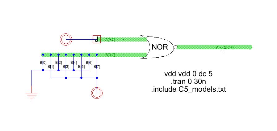
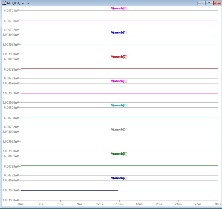
Figure 16: The simulation and results for the 8-bit NOR gate.
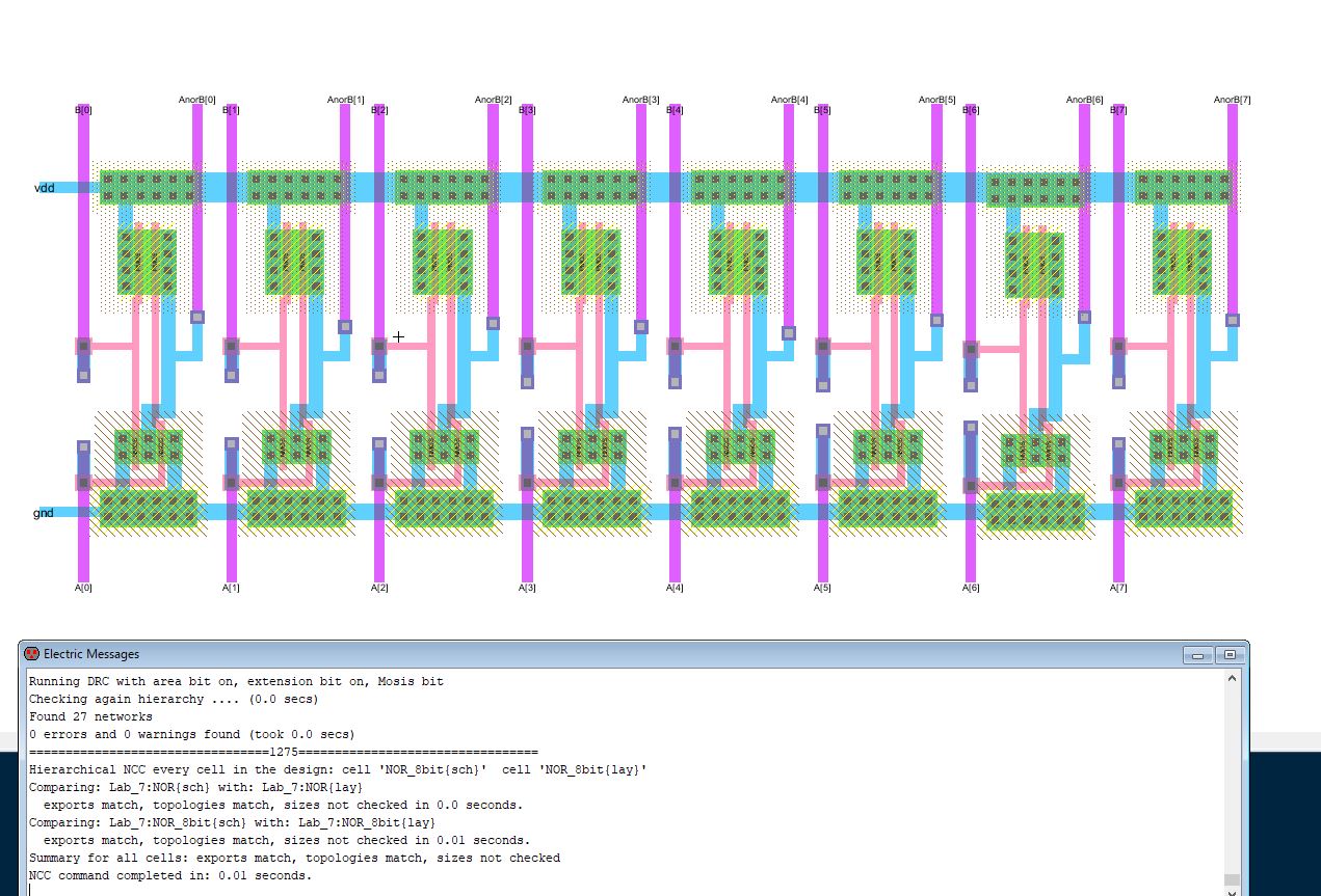
Figure 17: The 8-bit NOR gate layout with matching topologies and zero errors.
Lastly, the 8-bit NOR gate was simulated, Figure 16, with the results showing the expected logic. Once this was recognized, the layout was created and can be seen in Figure 17.
Figure 16: The simulation and results for the 8-bit NOR gate.
Figure 17: The 8-bit NOR gate layout with matching topologies and zero errors.
The objective of the lab was to use buses to create a ring oscillator and multi-bit logic gates. This lab though tedious, can be considered to be a success since the objective was fullfilled, the bus showed how much easier it is to simulate a multi-bit gate. Although a bus could not be used in the layout for each of the components, because each of the ports cannot be connected to each other.