Lab 6:
Build a NAND, NOR, XOR, and Full Adder
By: Roxie Sandoval
rlsandoval@fortlewis.edu
I. Introduction
The purpose of this lab was to build NAND, NOR, XOR, and a Full Adder using ElectricVLSI software.
II. Materials and Methods
i. Materials
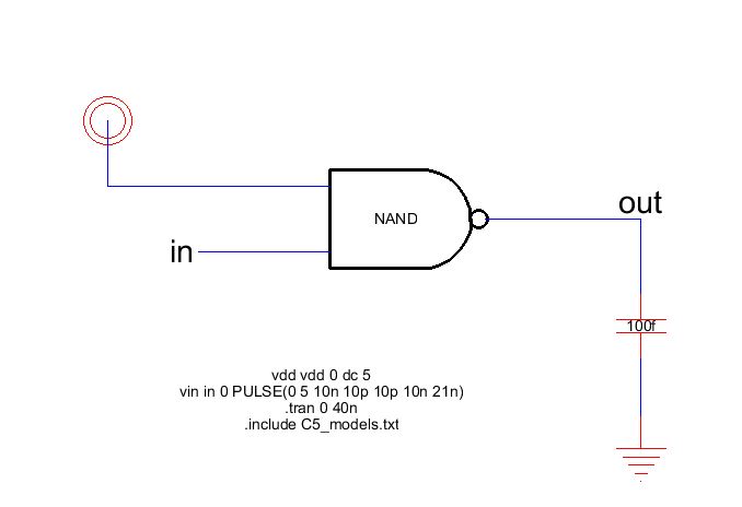
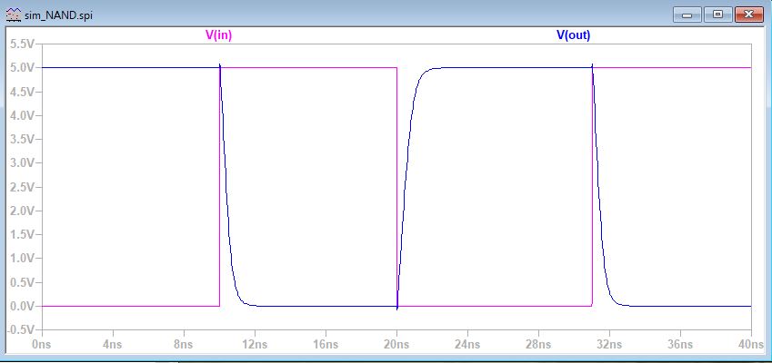
The NAND gate schematic was created and the icon was then created and this was then simulated in LTSpice, both the icon and the results can be seen in Figure 1, below. Once the logic gate was behaving as expected, the layout was created, because it will be used later in this lab, the layout had to have no errors and matching topologies and exports, as shown in Figure 2.
IV. Discussion
Though the lab was very tedious, it was an overall success, because each of the components used in the Full Adder had to have no errors and in the end had to be sized accordingly. The adder itself, had to be checked for errors as well, and ensuring these were addressed prior to moving on, greatly reduced the chances of mismatch topologies and errors.
The purpose of this lab was to build NAND, NOR, XOR, and a Full Adder using ElectricVLSI software.
II. Materials and Methods
i. Materials
1. ElectricVLSI software
2. LTSpice software
2. LTSpice software
ii. Methods
III. ResultsFirst
the schematics, icon and the layout for the NAND, NOR, and XOR logic
gates were created in ElectricVLSI. All were tested for errors and was
simulated in LTSpice for confirmation. Once all gates, were created and
tested , the schematic and icon for the Full Adder was created. The
adder, was simulated in LTSpice, once it was confirmed to be behaving
correctly, the layout was created and checked for errors.
The NAND gate schematic was created and the icon was then created and this was then simulated in LTSpice, both the icon and the results can be seen in Figure 1, below. Once the logic gate was behaving as expected, the layout was created, because it will be used later in this lab, the layout had to have no errors and matching topologies and exports, as shown in Figure 2.
(a)
(b)
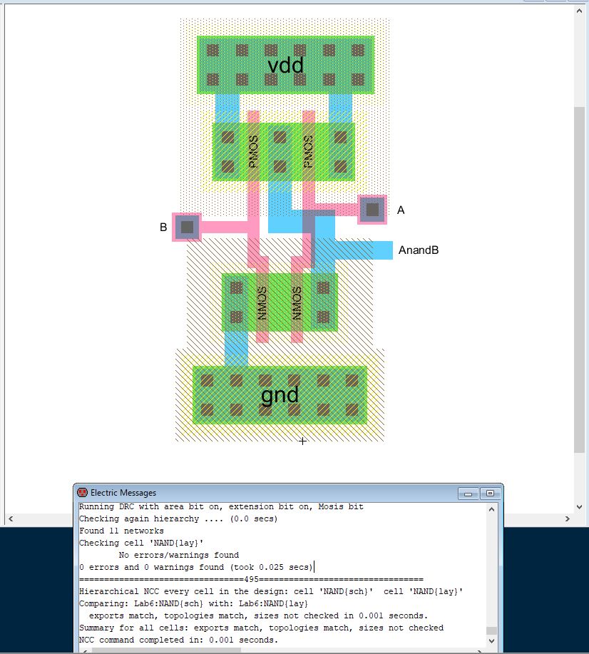
Figure 2: The NAND layout with zero errors and matching topologies.
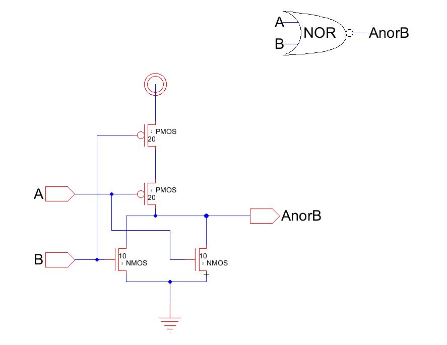
Figure 3: The schematic of the NOR gate and icon shown in the top right.
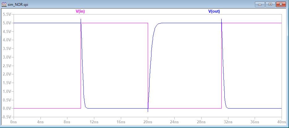
Figure 4: The LTSpice simulation results from the NOR gate.
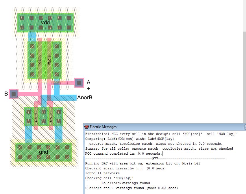
Figure 5: The NOR gate layout with clean DRC and matching topologies.
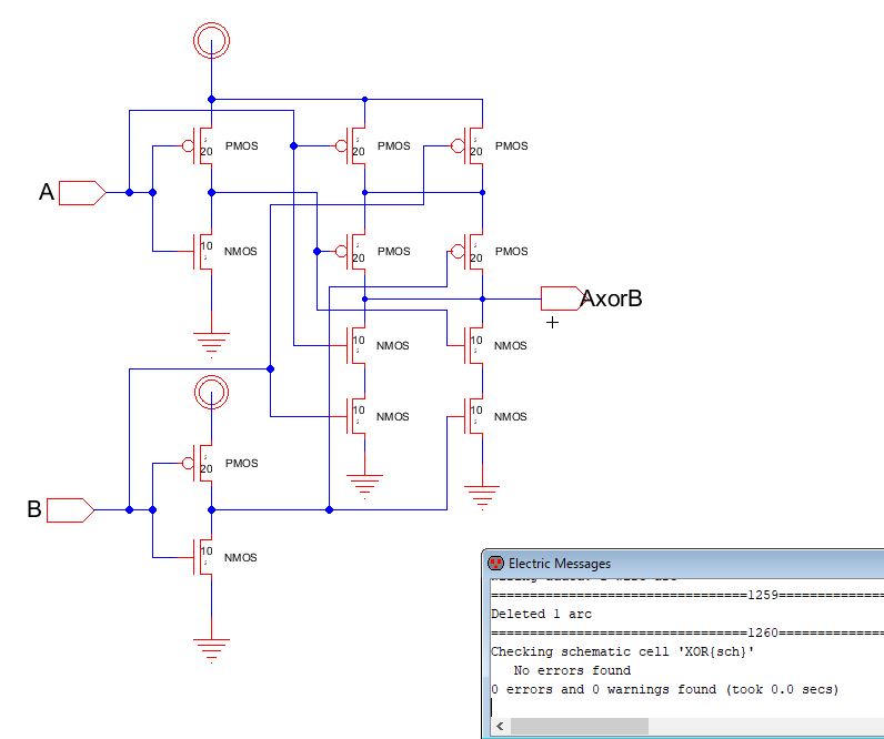
Figure 6: The schematic of the XOR gate with no errors.

Figure 7: One of the XOR simulations using the spice code given.
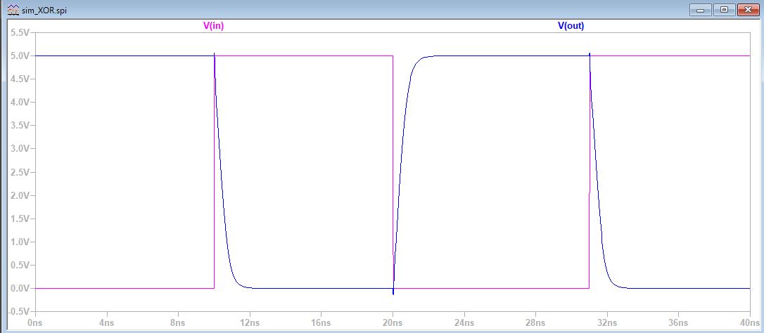
Figure 8: The results from the second XOR simulation, both behaved as expected.
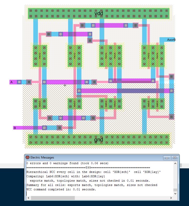
Figure 9: The XOR layout with clean DRC and matching exports and topologies.
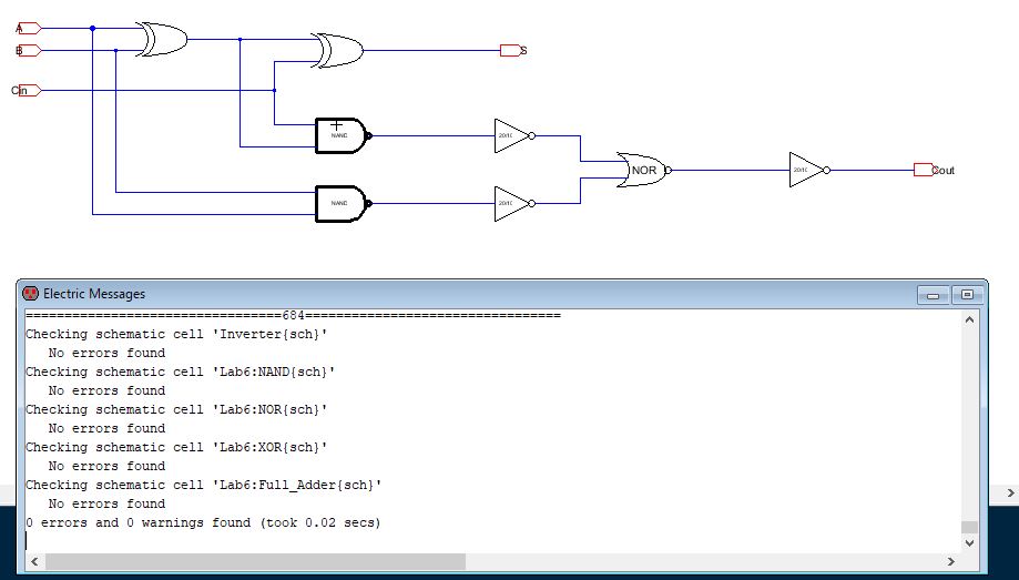
Figure 10: The Full Adder schematic, using the inverter from a previous lab and the logic gates created in this lab.
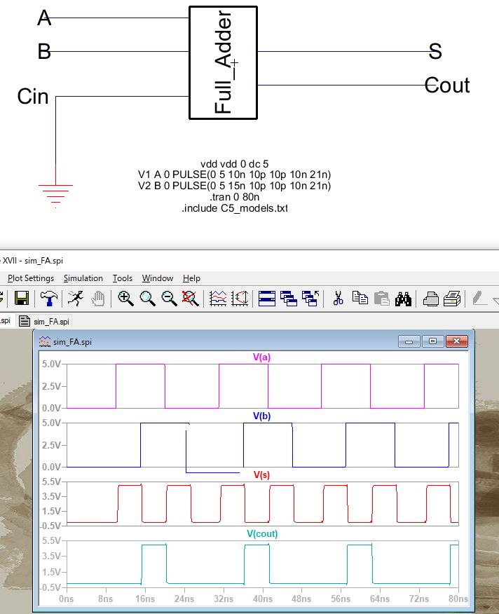
Figure 11: The Full Adder simulation using LTSpice, the results show the voltages at exports a, b, s, and cout.
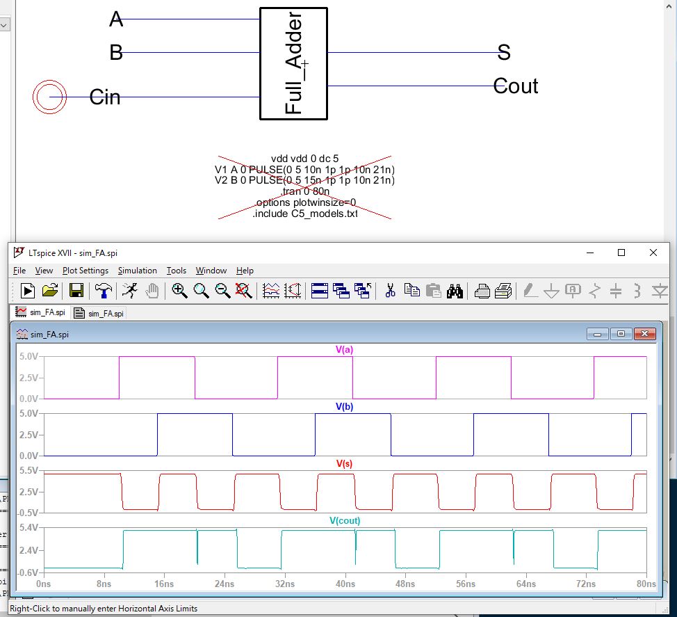
Figure 12: The second simulation Full Adder results.
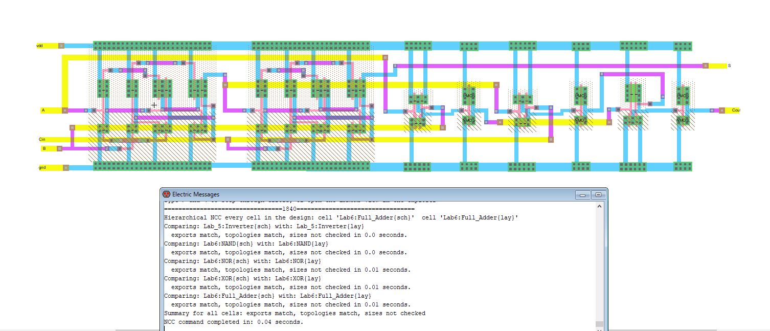
Figure 13: The Full Adder layout with zero errors and matching topologies.
Figure 1 (a): The NAND icon that was simulated in LTSpice. (b) The results from the simulation - which is what was expected.
Figure 2: The NAND layout with zero errors and matching topologies.
Next
the NOR gate schematic and icon was created, seen in Figure 3, this was
also simulated/tested in LTSpice, the results are shown in Figure 4. In
Figure 5, the layout of the NOR gate be seen, and shows clean DRC and
NCC.
Figure 3: The schematic of the NOR gate and icon shown in the top right.
Figure 4: The LTSpice simulation results from the NOR gate.
Figure 5: The NOR gate layout with clean DRC and matching topologies.
The
last logic gate to be created, that was used in the Full Adder, was the
XOR gate, a schematic of which can be seen in Figure 6. As previously
done, it was simulated twice in LTSpice, the results are shown in
Figure 7 and Figure 8, respectively. In Figure 9, the layout of the XOR
gate can be seen.
Figure 6: The schematic of the XOR gate with no errors.
Figure 7: One of the XOR simulations using the spice code given.
Figure 8: The results from the second XOR simulation, both behaved as expected.
Figure 9: The XOR layout with clean DRC and matching exports and topologies.
Lastly,
the Full Adder schematic can be seen in Figure 10, it integrated the
inverter from a previous lab, and XOR, NOR, and NAND gates from this
lab. The adder was simulated twice in LTSpice, both of which can be
seen in Figure 11 and Figure 12, respectively. Using the layouts from
each the logic gates, a layout for the Full Adder was created and
tested for errors and topological matches, this is shown in Figure 13.
Figure 10: The Full Adder schematic, using the inverter from a previous lab and the logic gates created in this lab.
Figure 11: The Full Adder simulation using LTSpice, the results show the voltages at exports a, b, s, and cout.
Figure 12: The second simulation Full Adder results.
Figure 13: The Full Adder layout with zero errors and matching topologies.
IV. Discussion
Though the lab was very tedious, it was an overall success, because each of the components used in the Full Adder had to have no errors and in the end had to be sized accordingly. The adder itself, had to be checked for errors as well, and ensuring these were addressed prior to moving on, greatly reduced the chances of mismatch topologies and errors.