Lab 5:
The Inverter
By: Roxie Sandoval
rlsandoval@fortlewis.edu
I. Introduction
The objectives of this
lab was to be able to design and build a layout of an inverter in Electric and simulate in LTSpice.
II. Materials and Methods
i. Materials
1. Electric VLSI software
2. LTSpice software
ii. Methods
First the schematic of the inverter was created, this was then created into
an icon and DRC checked. Once this is error free, it was simulated using LTSpice. Secondly, a layout of the inverter was built, this too was checked for errors and hierarchical errors. Then
using the inverter and adding a multiplier both to create a larger
inverter by adding 5 PMOS and NMOS in parallel. This was also checked
for errors and matching topologies. Once this is error clean, the 20/10
and 100/50 inverters were then simulated in LTSpice with 100fF,
1pF, and 10pF capacitors.
i. Task 1
Figure
1, below shows the first task result simulation with the output signal
was inverted as expected. The pulse simulation in Figure 2 shows the
inverted output signal.
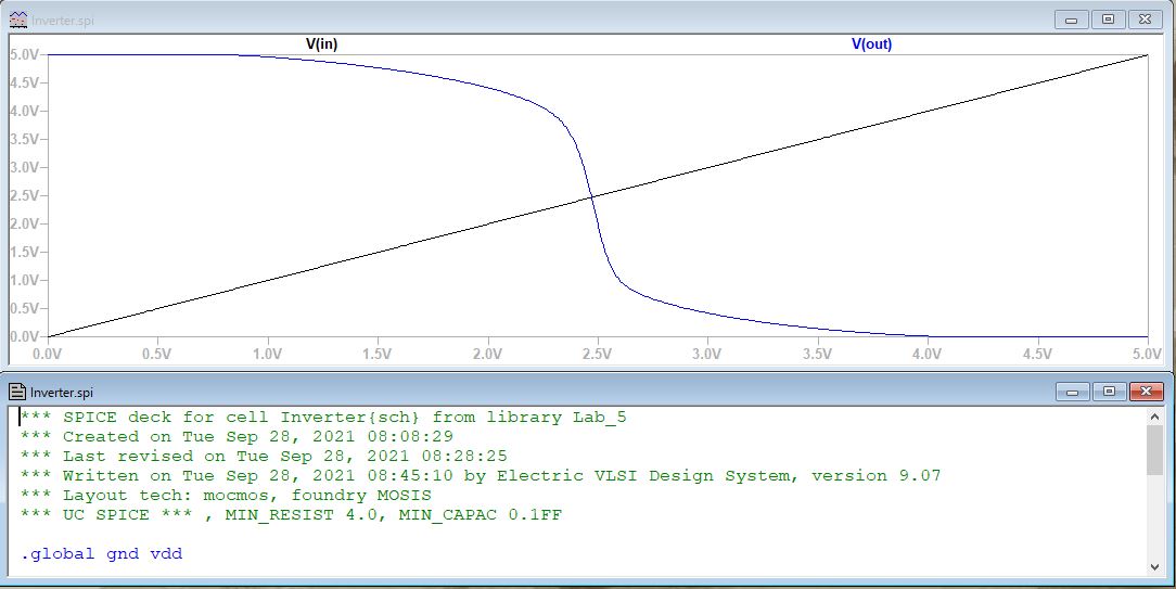
Figure 1: The first simulation showing the inverter, inverting the output signal.
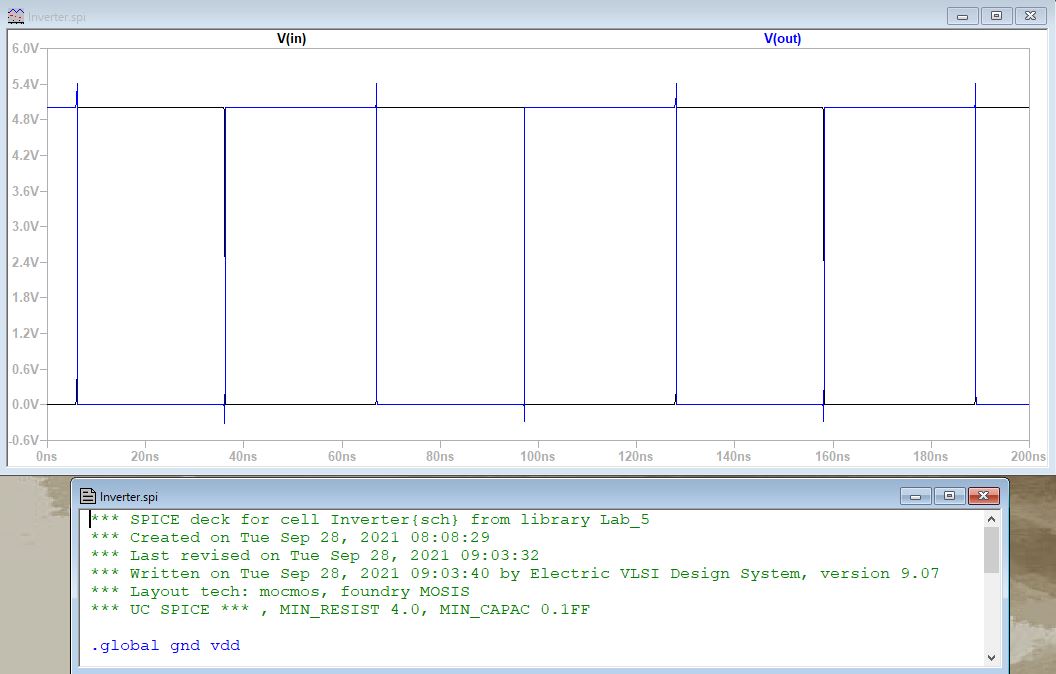
Figure 2: The pulse simulation for the inverter.
ii. Task 2
The layout of the inverter can be seen below in Figure 3, with a clean DRC and LVS, showing matching topologies and exports.
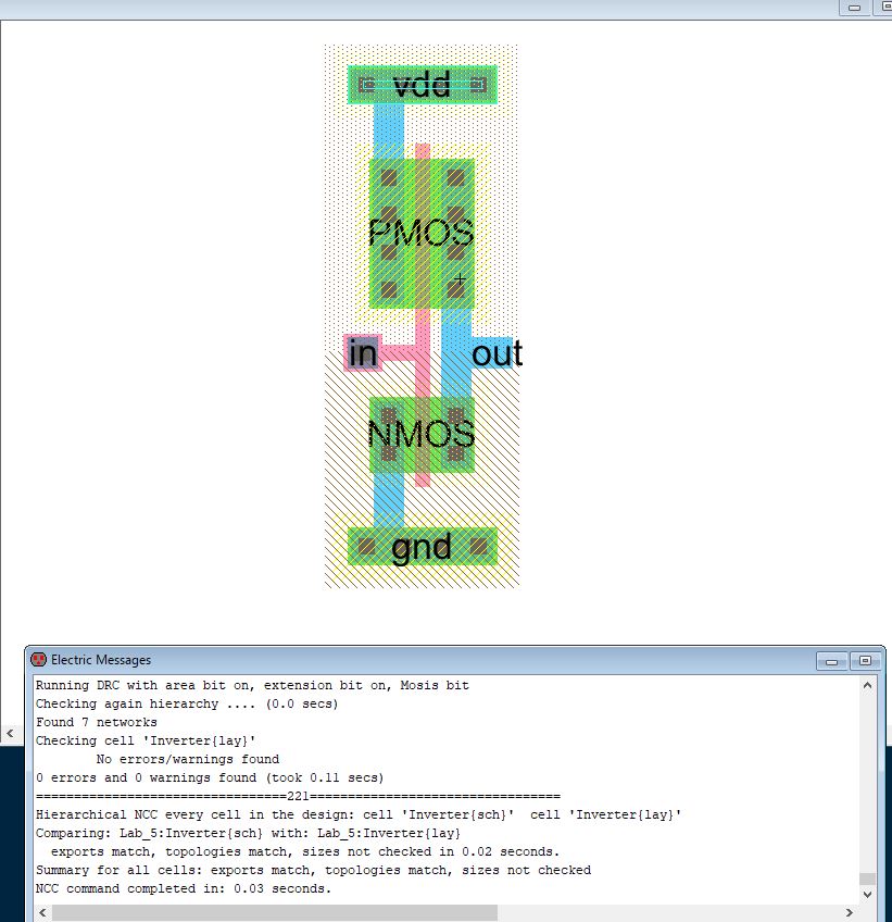
Figure 3: The layout of the schematic with no errors and matching topolagies.
iii. Task 3
Using
the previous inverter layout, a larger inverter was created as seen
below in Figure 4, This was also checked for errors and matching
topologies.
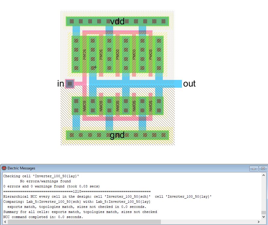
Figure 4: Larger inverter with clean DRC/LVS.
iii. Task 3
Figure
5 below shows the 20/10 inverter with a 100fF capacitor simulation with
the inverting output. The same inverter was simulated using a 1pF and
10pF, both are shown in Figure 6 and Figure 7, respectively.
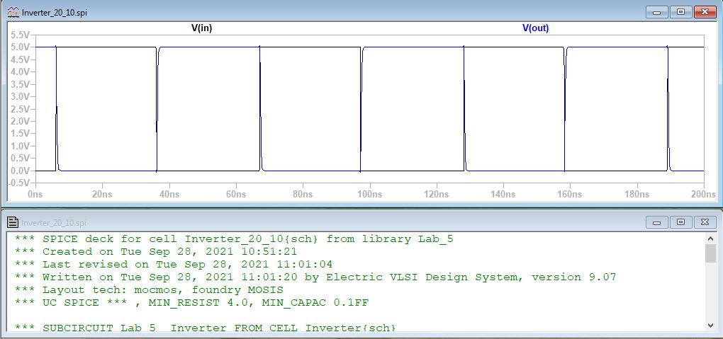
Figure 5: The 20/10 inverter with the 100fF capacitor simulation.
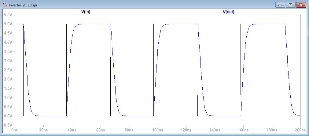
Figure 6: The 20/10 inverter simulation with the 1pF capacitor.
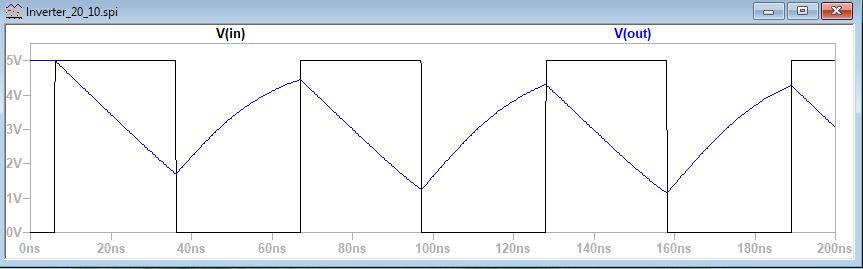
Figure 7: The 20/10 inverter with a 10pF simulation.
Figure 8 below shows the larger 100/50 inverter simulated with a 100fF capacitor, showing the inverted output signal.
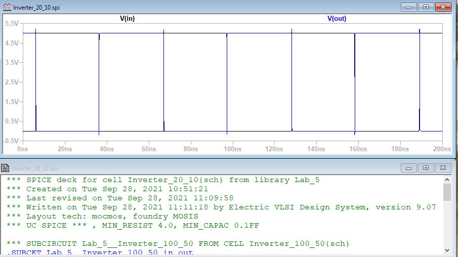
Figure 8: The 100/50 inverter simulation with 100fF capacitor.
The same large inverter was simulated with 1pF and 10pF capacitor in Figure 9 and Figure 10, respectively.
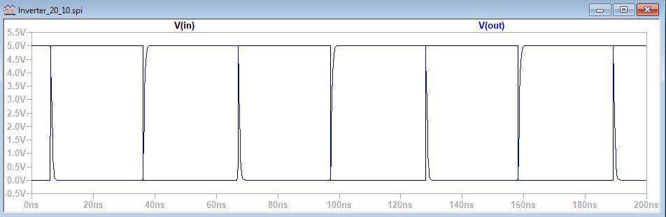
Figure 9: The 100/50 inverter with 1pF capacitor simulation.
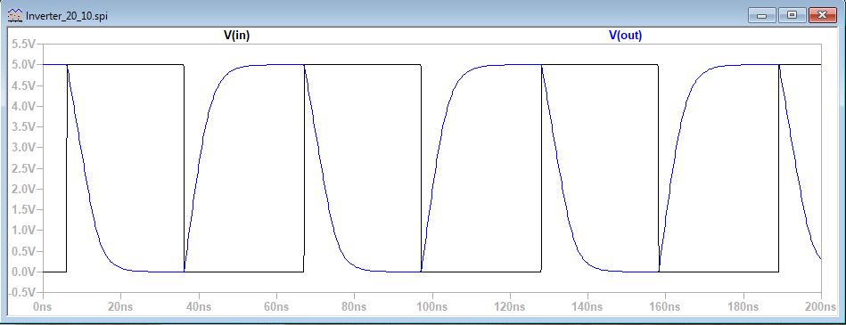
Figure 10: The 100/50 inverter with the 10pf capacitor simulation.
IV. Discussion
Each
of the simulations showed the output signals were inverted therefore
proving both the schematics and layouts worked as expected. Not only
did they show the inverted output but they also showed how it could be
modified within a circuit, such as increasing the capacitance. The
simulation also showed that the smaller inverter allowed for less
current which kept the capacitor from completely charging.