ENGR 338 - 2021 Fall
Lab 4:
MOSFETs and IV Curves
By: Roxie Sandoval
rlsandoval@fortlewis.edu
I. Introduction
The objectives of this
lab were to build MOSFETs in Electric and use LTSpice to simulate and
analyze the current-voltage (IV) curves.
II. Materials and Methods
i. Materials
1. Electric VLSI software
2. LTSpice software
ii. Method(s)
First the schematics for both
the NMOS and the PMOS were created in thier individual cells, then they
were modelled with LTSPice - this will allow both to be simulated in
LTSpice. Once
both had thier schematics created, thier layouts were designed, during
the process well and error checks were conducted. When the layouts were
completed, a spice code was written to allow the NMOS and PMOS layouts
to simulated separately.
With a successful simulation, the schematics were then redesigned to
match the layout of both NMOS and PMOS. Like the layout procedure -
these required error checks, if there were no errors they were
simulated, again, in LTSpice.
III. Results
i. NMOS
The NMOS layout was designed and can be seen in Figure 1, below. The
NMOS had to be checked multiple times for design errors, so it can be
successfully simulated in LTSpice. After simulation, the schematic was
designed to have matching ports which can be seen in Figure 2. The
figure also included the Spice code used in both simulations.
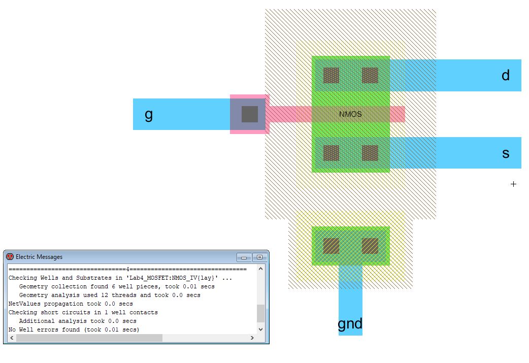 Figure 1: The layout of the NMOS, with no well errors.
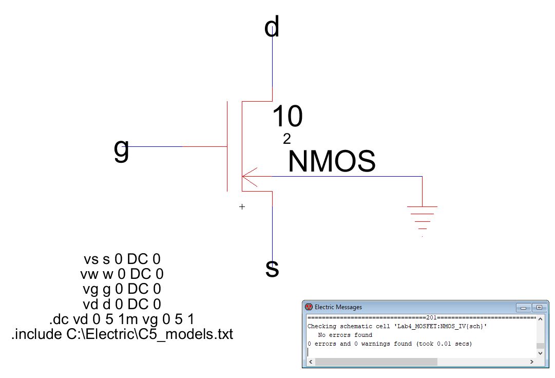 Figure 2: The NMOS schematic with matching ports and clean DRC, with the Spice code.
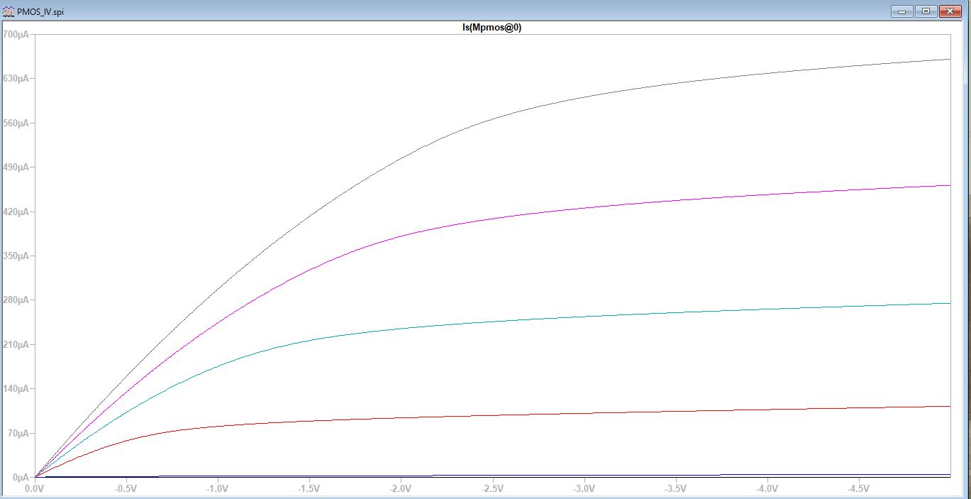
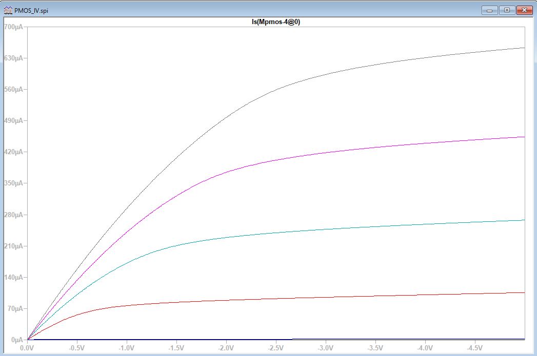
Figure
3 and Figure 4 below show the resulting simulations from the layout and
schematic designs, respectively. The results from the layout simulation
was taking from the source or "s" port from the previous NMOS layout
figure.The results from the schematic was simulated from the drain (d) port, shown in Figure 2.
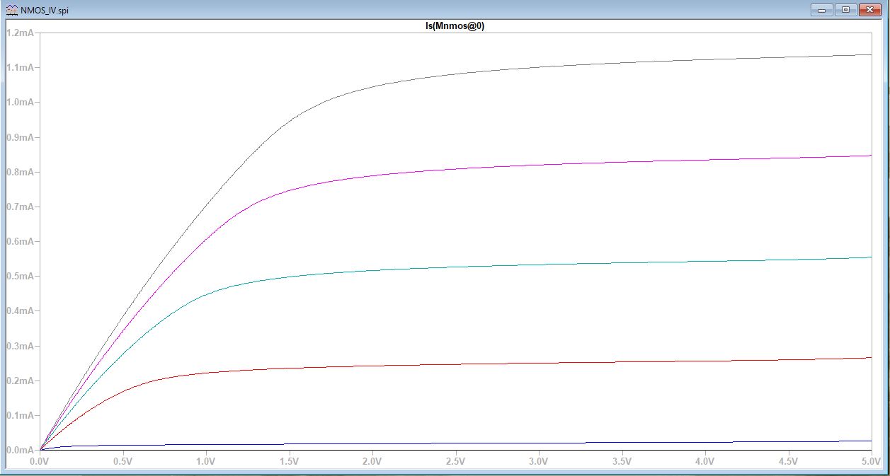
Figure 3: The NMOS layout simulation results, taken from the source port.
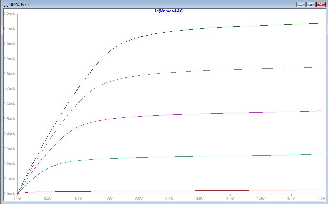 Figure 4: The simulation results from the NMOS schematic, taken from the drain port.
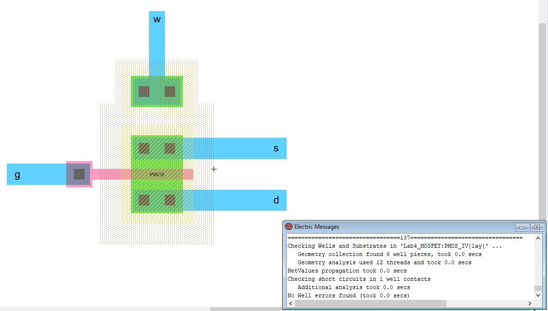
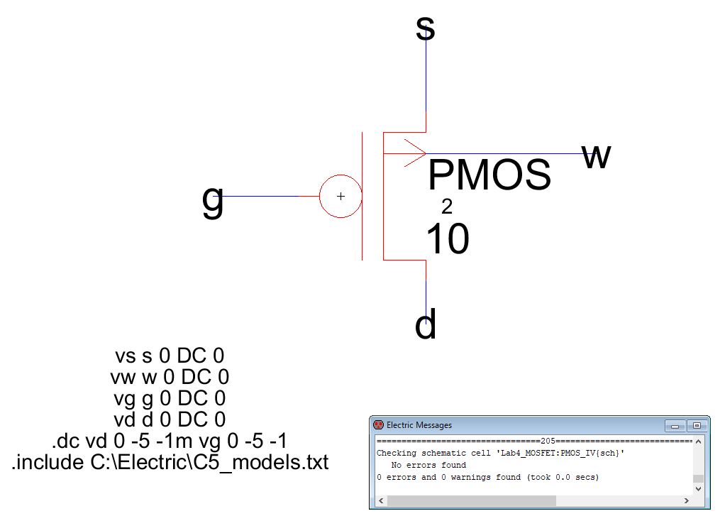
ii. PMOS
As for the PMOS, similar procedures were followed and therefore Figure 5, below shows the layout with no well errors, as well. Then the schematic of the PMOS was designed and DRC or error checked, Figure 6.
IV. Discussion
This lab was proven to be successful with the proper simulation
results. Both the NMOS and PMOS had the same results for both thier
layout and schematic designs which was expected.