Figure 1: The R-2R ladder icon, with a clean DRC.
Since
the subcell icon was clear of errors, it was then copied and paste to
create the ladder like that seen in Figure 2, this too needed to have a
clean DRC. This would be used in task two in this lab.
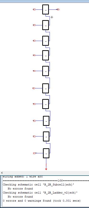
Figure 2: The ladder created by the subcells with a clean DRC.
ii. Task 2
Figure 3, shows the n-well resistors laid out similar to the repeating resistors structure, this was also connected to create a ladder, like that in Figure 4.
Figure 3, shows the n-well resistors laid out similar to the repeating resistors structure, this was also connected to create a ladder, like that in Figure 4.
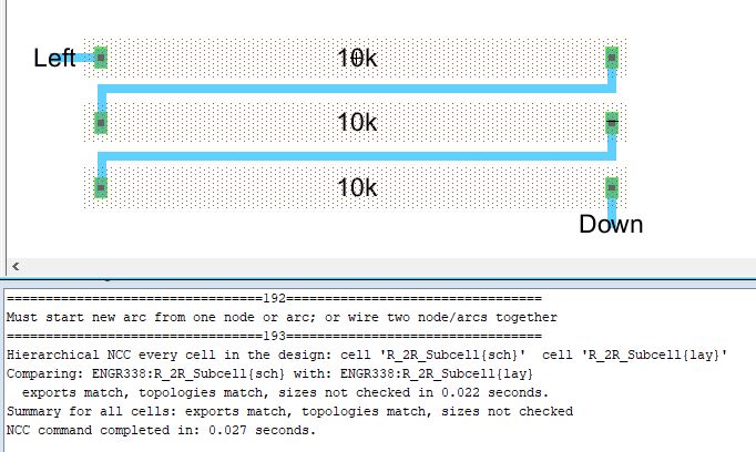
Figure 3: The n-well resistors laid out like the subcell resistors, with a clean DRC.
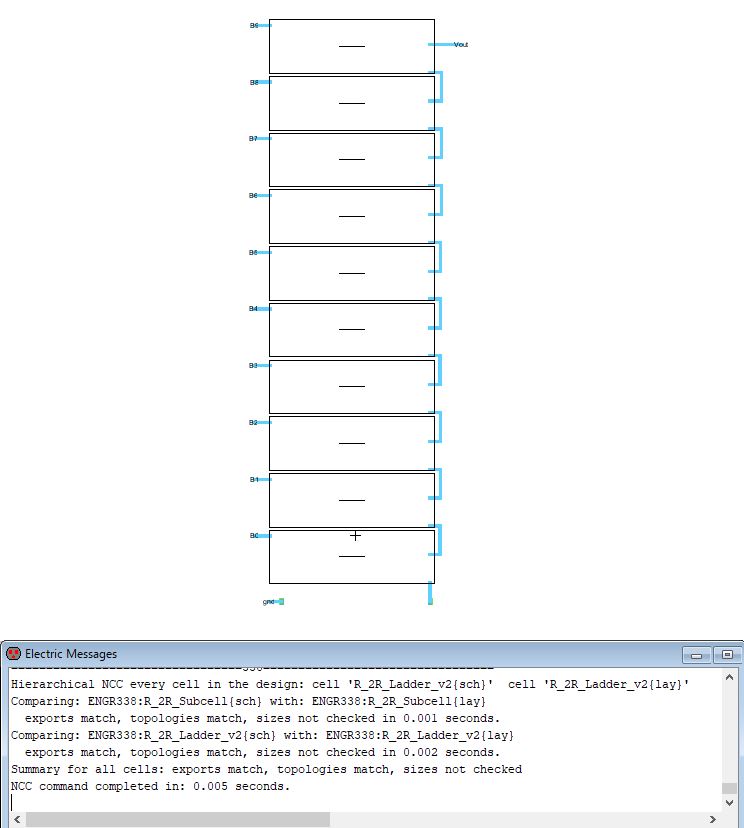
Figure 4: The n-well resistors connected - creating R-2R ladder, with a clean DRC/LVS.
When the DRC/LVS was shown to have zero errors and topologies matched, it was connected to the ideal ADC, as shown in Figure 5.
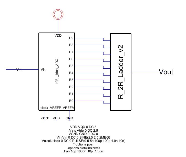
Figure 5: The R-2R ladder paired with the ideal ADC.
This was simulated in LTSpice, it compared the Vin and Vout shown in pink and blue respectively in Figure 6. The simulation proved the R2-R ladder behaved and worked as expected.
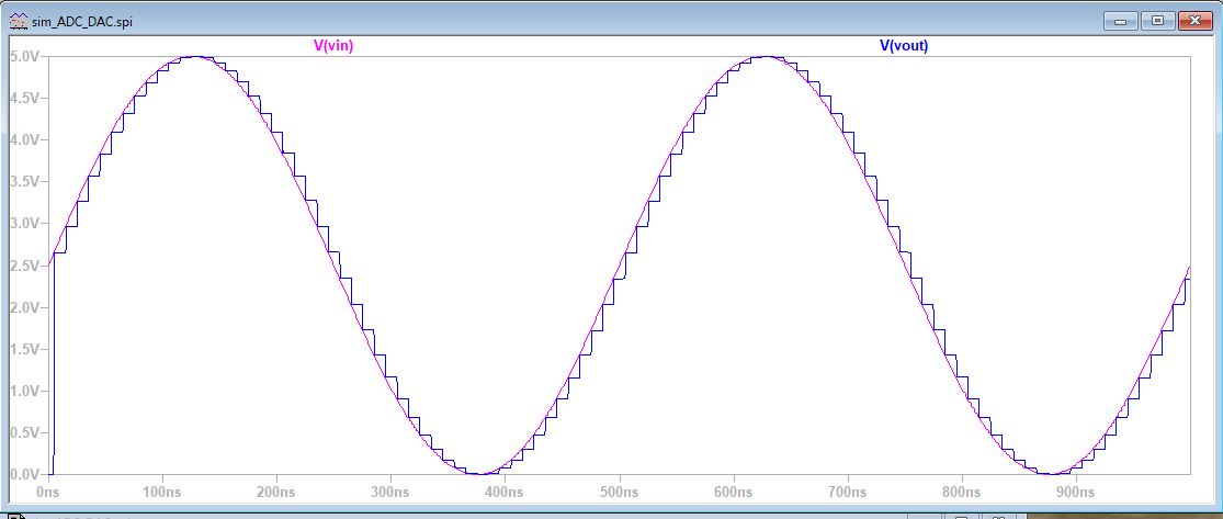
Figure 6: Resulting simulation from the R-2R ladder.