ENGR 338 2021 Fall
Lab 2 :
Design an R-2R DAC
By: Roxie Sandoval
rlsandoval@fortlewis.edu
I. Introduction
A R-2R resistor ladder network converts a digital word or symbol to an
analog voltage. The objectives of the lab were to understand the
operation of an ideal ADC and DAC, and design a R-2R resistor ladder in
Electric VLSI. Both objectives will allow a familiarity to use Electric
VSLI and LTSpice for integrated circuits.
The first objective, an ideal ADC/DAC was given and tested using
LTSpice. As for the second objective, a R-2R resistor ladder network
was required to be created in Electric and was tested also using
LTSpice.
II. Materials and Methods
i. Materials
1. Electric VLSI software
2. LTSpice software
3. Paper
4. Pencil
i. Methods
Before each of the tasks were started, the configuration for Electric and LTSpice were completed. Then for task one, an ideal ADC/DAC was already designed and available for download, therefore it was
downloaded and a Spice Deck was written for testing. Once recieving the
expected Vin-Vout simulation, a R-2R resistor ladder network was then
designed in Electric software. To ensure all connection were correct,
the schematic must first be DRC clean, then it was converted to an
icon. The R-2R icon was then connected to the ideal DAC and simulated
in LTSPice, as well.Lastly, the time delay on the R-2R ladder was tested and compared to hand calculations.
III. Results
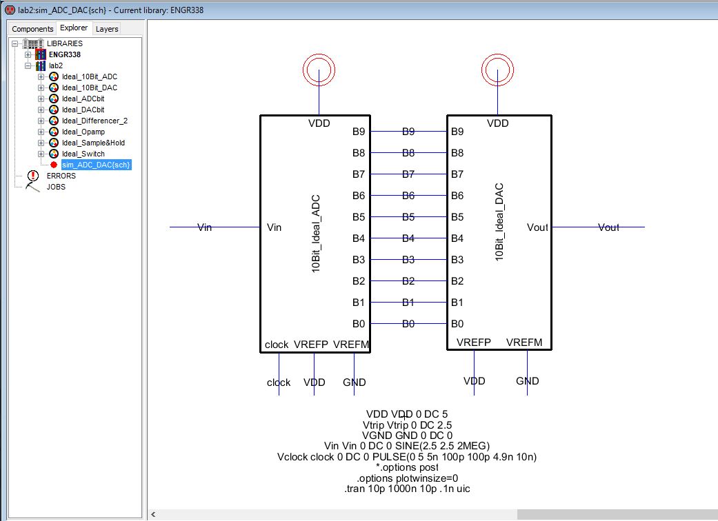
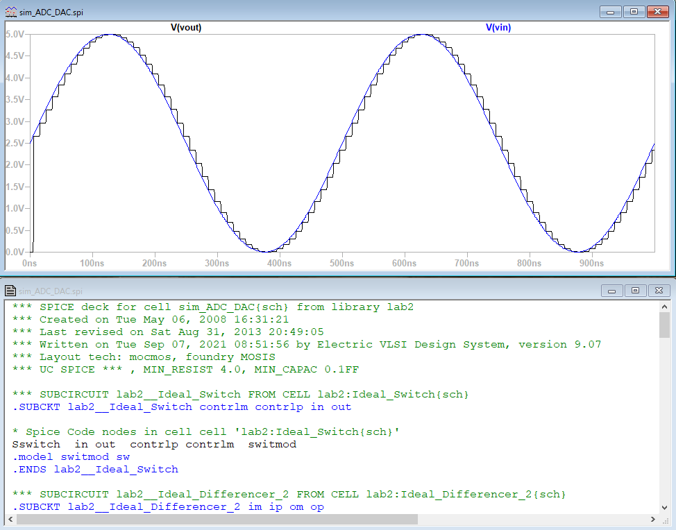
i. Task 1
To
ensure Electric and LTSpice were properly configurated, the ideal
ADC/DAC icons which can be seen in Figure 1(a) was simulated in LTSpice, Figure 1(b). The Vin-Vout simulation behaved as expected, with a sine wave input and the stair-like output.
(a)
(b)
Figure 1 (a): The ideal ADC and DAC that was tested using LTSpice. (b) The resulting simulation from the ADC/DAC.
ii. Task 2
Because
both softwares were behaving coherently, the second task of
constructing the R-2R ladder began which can be seen in Figure 2.
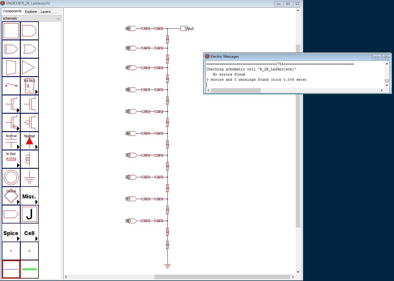 Figure 2: The R-2R ladder network that was designed and shown to have a clean DRC.
The ladder was then converted to an icon that was to be connected to the ideal ADC, as shown in Figure 3.
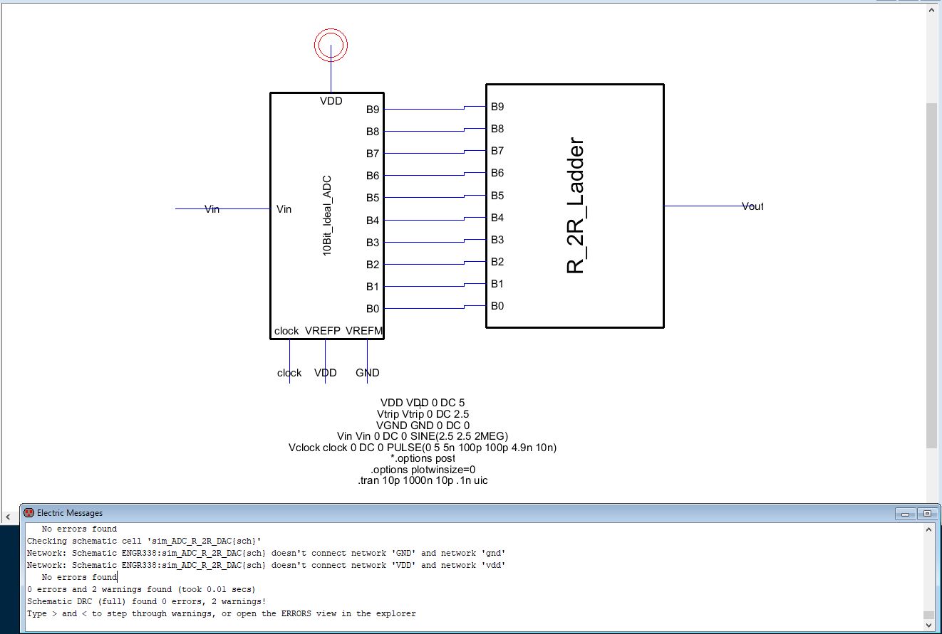 Figure 3: The R-2R ladder icon connected to the ideal ADC, with a clean DRC.
From
the above configuration, Figure 4, shows the simulated input and output
in Spice, which resulted in a similiar Vin-Vout graph as the ideal
ADC/DAC.
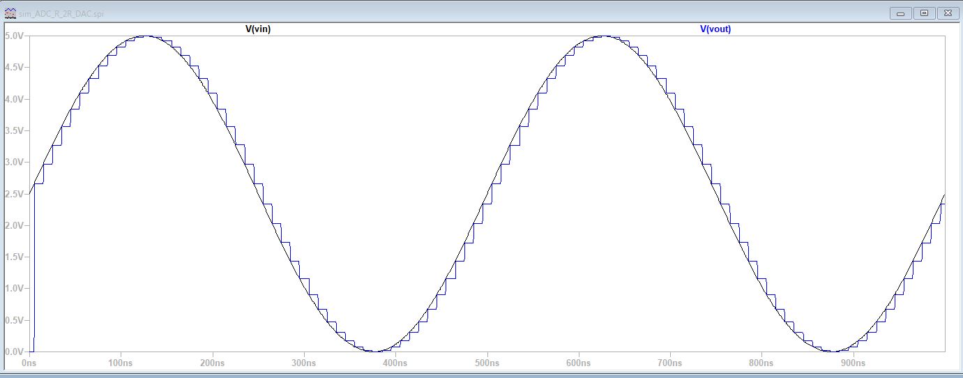 Figure 4: The resulting simulation from the R-2R ladder and ideal ADC - shows the input as a sine wave and the step-like output.
iii. Task 3
Last
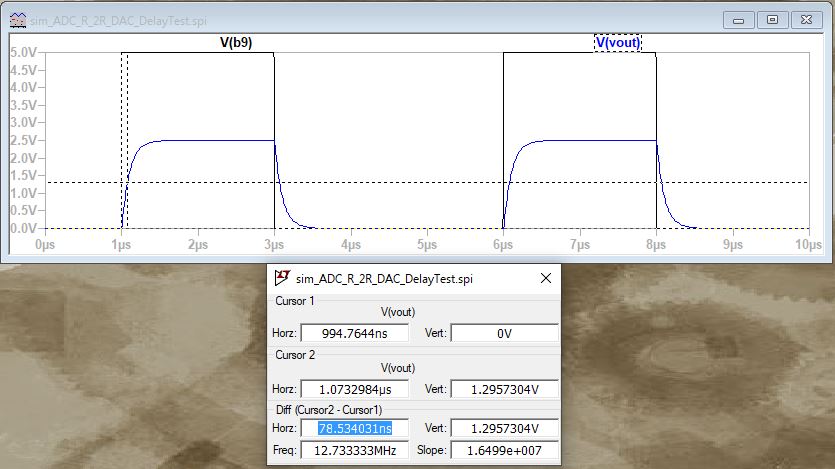
task of the lab, checked the time delay of pin B9, as shown below in
Figure 5. The figure shows the icon view of the ladder, with all pins
except pin B9 grounded. This also had a 10pF capacitor at the Vout
creating a RC circuit.
 Figure 5: The R-2R ladder with the B9 pin connected to a pulse, to test the time delay.
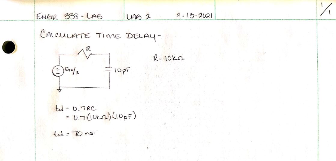
The
RC-circuit resulted in a time-delay of 78.5ns and a Vout of 1.29V,
Figure 6(a) - this is close to the hand calculated time delay equal to
70ns. Figure 6(b) shows the calculations for the simple RC-circuit,
where Vout was expected to be a half of VDD (2.5V), therefore 1.29V is
considerbly close to 1.25V.
(a)
(b)
Figure
6 (a): The Vin-Vout simulation, where pin B9 was the input, it showed
the Vout was approximately half of the VDD and the time delay as
78.5ns. (b) The hand calculations that showed the time delay was found
to be 70ns - close to the simulation.
IV. Discussion
Each
of the objectives of this were completed, which proved this to be
successful. Figure 1 showed a successful import and simulation of an
ideal ADC/DAC and figure 2 through 4 shows the creation and results of
the R-2R ladder. Lastly, figures 5 and 6 shows the comparisons in the
time delay calculations.