Week 2 Homework
Noah
Smith
1. Work on the following problems: (20
points)
2. Repeat the simulation work in Section 5. Demonstrate your results in
embedded videos on your website. (20 points)
This task from section 5 was straight forward with the
tutorial. Code and simulation results can be seen below.
3. Repeat all the FPGA experiments in Section 7. Demonstrate your results in embedded videos on your website. (30 points)
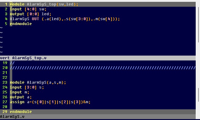
Alarm system:
This system was relatively easy to implement. The only
challenge I ran into was having two different simulation/synthesis files, which
caused errors when trying to write the bitstream. Once that was sorted out it
worked perfectly and can be seen in the embedded video below. The code is included
below as well.
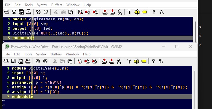
Password:
This password/digital safe system was really
cool to implement. I left the password the same as the example (0101).
Writing bitstream went smoothly and you can see the embedded video for this working
as well as the code used.
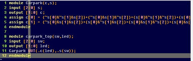
Car Park:
The car park logic seemed
similar to a digital counter to me. I demonstrated it
matching the truth table in the embedded video and the code can be seen below.

4. Design a simple digital system using the similar combinational logic design
methods shown in Section 7. Explain what the system is, show the design files,
demonstrate it on your FPGA. Demonstrate your results in embedded videos on
your website. (30 points)
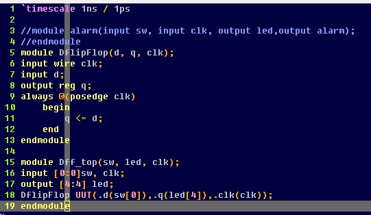
The simple digital system I chose to design was a D flip-flop.
This didn’t exactly use combinational logic but I thought
it would be a nice challenge. The trickiest part was figuring out how to implement
the clock built into the board. This was done by calling its port (clk) and using
behavioral coding, where you set the trigger on the rising edge of the cycle. From
here it was a simple matter of using blocking assignment to pass D to Q. The
video demonstration doesn’t look very impressive as the clock cycle built
into the board with a crystal oscillator
is at a 100Mhz frequency and is too fast for humans to see. But looking at the
code you can see that the data input switch is not bound to the Q output
anywhere except for on a rising clock edge. In the video I have SW[0] bound to Data and LED[4] set as the output. To improve
this you could obviously add set and reset inputs, as
well as creating a custom digital clock and slowing the frequency down to see
the logic happening. Code is below.