Course
Project: SAR ADC
Noah Smith
This project has several key parts:
·
SAR
·
Sample and Hold Circuit
·
Operational Amplifier
·
Door and Clock register
·
Digital to analog converter (DAC)
This project will be completed in Electric VSLI
and simulated in LTspice.
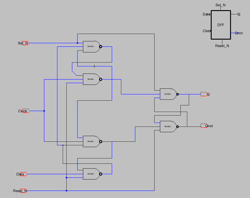
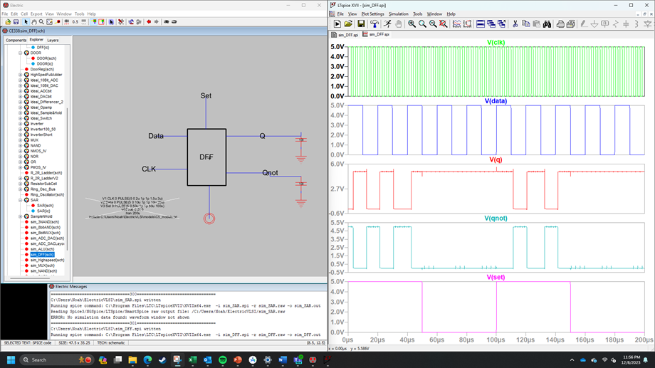
A few elements of this circuit need to be
created before the fun work can start, the Data Flip Flop and the Buffer. This
is a flip flop circuit that passes data. This needed to be built in Electric VSLI. The schematic and simulation can be seen
below.
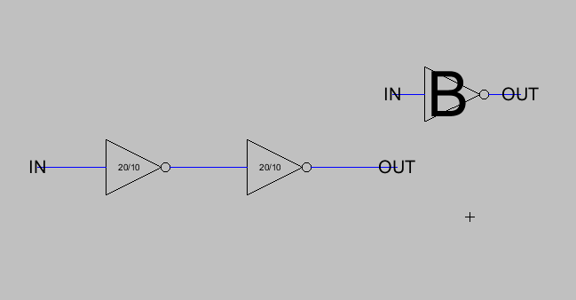
Creating the buffer was a simple matter of
chaining two inverters together to create a noninverting buffer, this can be
seen below. I used an already existing inverter design to achieve this.
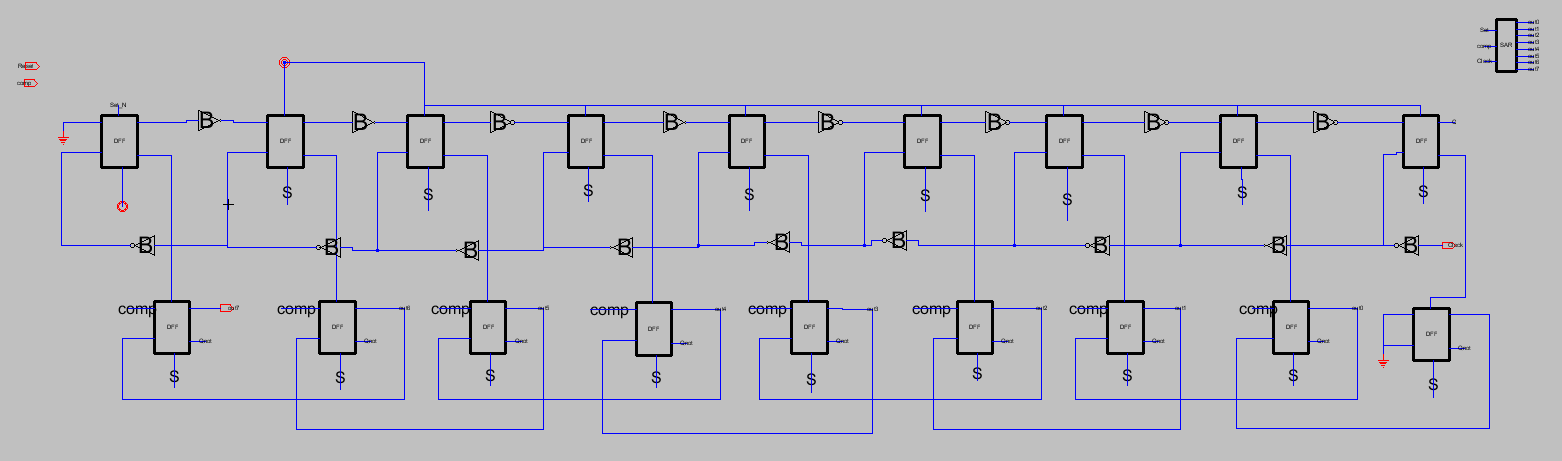
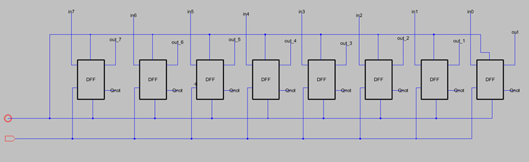
SAR:
The first part of this project is creating the
SAR logic. This was done by laying out a grid of DFF’s and wiring them
together, carefully following the design. The schematic of this and an
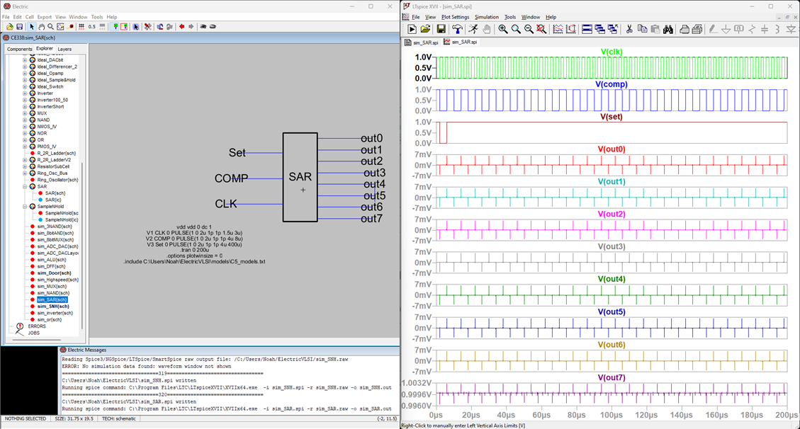
attempted simulation can be seen below. It must be noted that a proper working
simulation for the SAR was never achieved. This is despite weeks of
troubleshooting and several ground up rebuilds of the
circuit. Going as far as rebuilding the NAND gates, inverters, DFFs and the SAR
circuit itself. Everything was checked and double checked to no avail. I went
as far as looking at and ensuring matching connections to classmates’ circuits.
Still no success.
I have provided the failed simulation and spice
code used to run it. If any errors are obvious please
reach out.
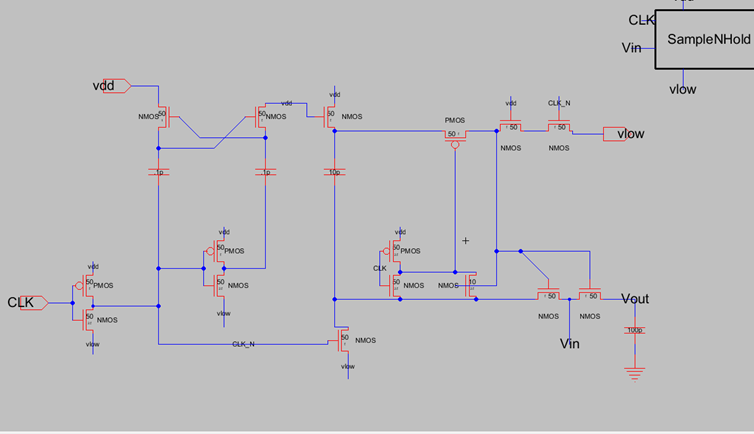
Sample and
Hold circuit
The sample and hold circuit is
a critical component of the circuit. Its purpose is to sample an analog input
and hold that voltage long enough for the SAR circuit to convert to a digital
signal.
The schematic can be seen below. This was
carefully adapted from the LTspice circuit in the
instructions.
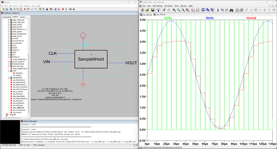
The simulation of the sample and hold circuit
is not perfect as the data from the upper ¼ of each wave is lost. I
troubleshooted this by checking and changing spice code, playing with the sizes
of all the transistors and capacitors involved in the circuit to no avail. This
was the best I could get this simulation.
OP AMP
The OP amp and biasing circuit from this lab come
from the opamp.zip file provided for the project. I was unable to get any of
these to open or work in Electric VSLI, but given that
none of the other simulations for this project work, the final sim is doubtful
to work and I chose to use the ideal op amp that was preloaded into the
Electric VSLI library I was using as a placeholder.
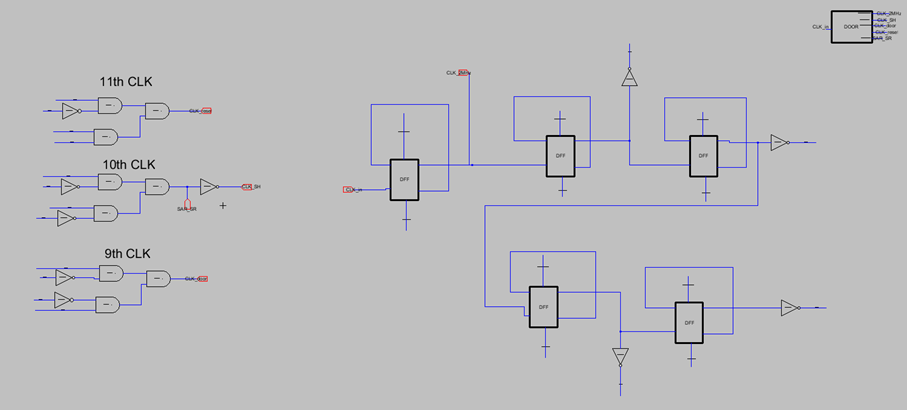
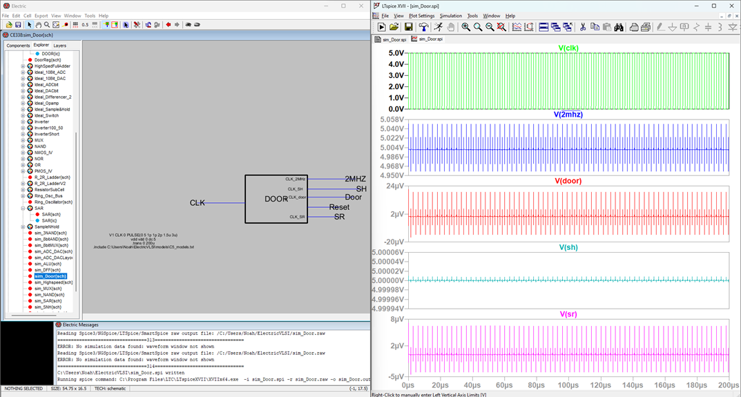
DOOR and
Clock Register
This set of circuits is critical to the
operation of the circuit. It is the timing for the whole circuit. The schematic
for the 4 parts of this circuit can be seen below as well as
yet another failed simulation. An equal amount of troubleshooting was
applied to this circuit as well, to no avail. All circuits were copied as
exactly from the instructions as possible and verified against classmates’
designs. No idea why it does not work. As shown the
simulation only provides noise for the output clock signals. These should be
clock signals that trigger on the 9th, 10th
and 11th input clock signals. The schematic for the door register is
also provided.
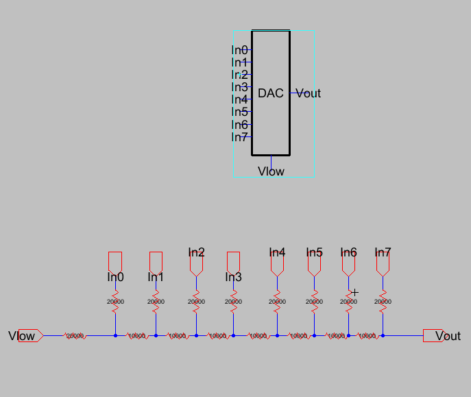
DAC
The DAC part of this project was a simple
matter of lining up some resistors and exporting pins. Nothing hard here.
Schematic seen below.
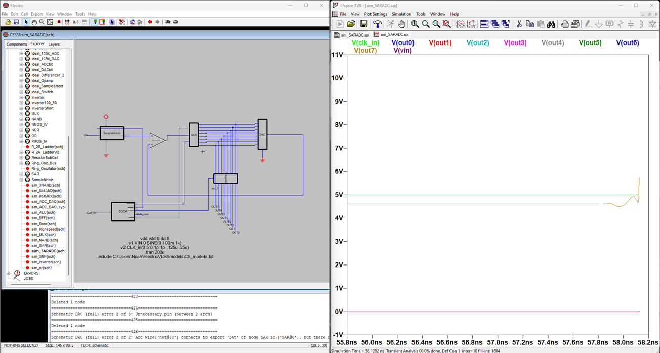
Full
Circuit & Conclusion
Below is the schematic of the full circuit and
a failed simulation of the circuit. The second DAC was omitted from the final
design as it is purely there for check purposes. As expected from the above
report, this simulation does not work. This is likely due to some root problem
with the SAR and all other failed simulations. As mentioned above, I have spent
weeks trying to troubleshoot these issues to no avail. I have checked the
functionality of everything down to the 3 input NAND gate and that logic works.
Given that the DFF logic also works it leads me to believe that the error for
the SAR at least lies in the SAR circuit, but as mentioned this has been
rebuilt many, many times and checked and double checked for the smallest
differences between my circuit and the instructions/classmates
circuits. The same approach was used for troubleshooting the other circuits. If
any errors can be identified from this report please reach out.