Noah Smith
The purpose of this lab is to create a MOSFET transistor
using the electric VSLI program. We created both a schematic and physical
layout for and NMOS and PMOS transistor.
Below are each of the schematic views created
for the NMOS and PMOS transistors.
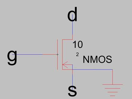
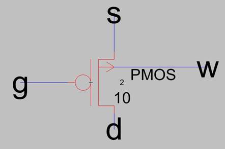
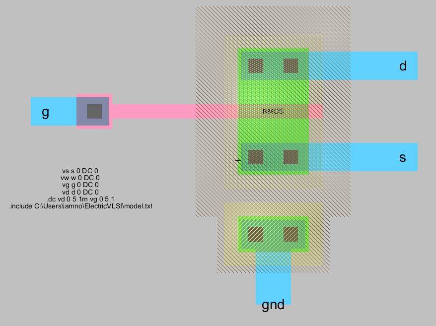
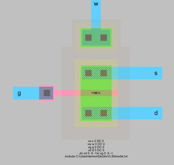
Next we needed to create the physical layout of the transistors. The
next two pictures show what NMOS and PMOS layouts look like. The different
hashmarks indicate the doping of the silicon that these wells would be
fabricated on. The blue areas represent the different leads of the transistor,
Gate, Drain, Source and Ground.
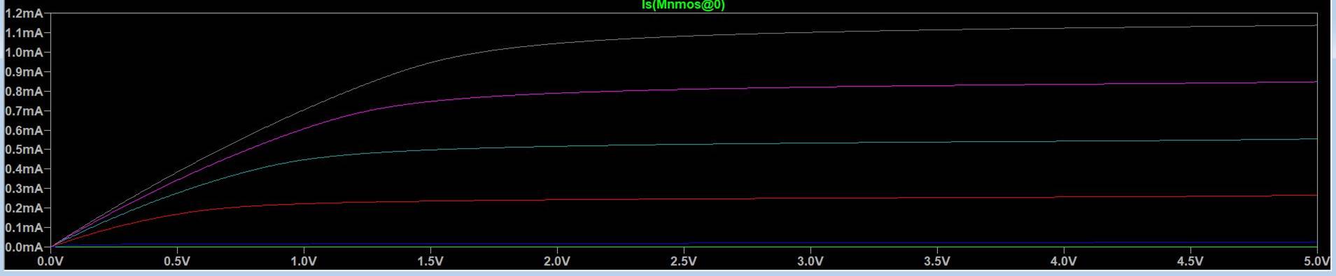
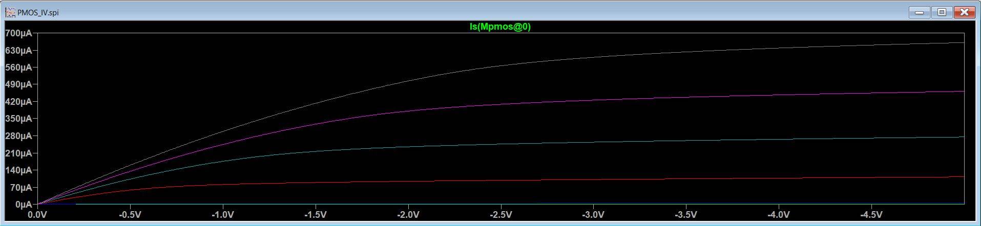
Below are the simulation results for simulating
both transistors in LTspice. The pretty curves are created because we vary the
voltage of the drain from 0 to +/- 5v in increments of 1mV and then change the
voltage at the gate by 1 volt. Each line represents a different gate voltage.
The top picture is NMOS and bottom PMOS