Lab 2
Noah Smith
Task
1: Copy the existing ideal ADC-DAC files to your ENGR338 library and run the
simulation.
Notes on Electric VLSI setup:
-Save the Electric VLSI .jar file to C:\Users\yourname and
create a folder there for it.
-Save the Lab2 library to the above folder.
- If there are File path issues, try a fresh install of LTspice and use the default file path.
Once Electric VLSI was
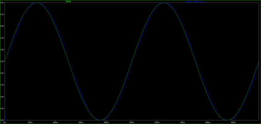
properly setup, the example ADC_DAC circuit was simulated using LTspice. The output is as follows:
.
In this output you can see the analog input
signal in green, and the stepped digital output signal in blue. It looks this
way because of the resolution that a 10bit ADC can provide.
Task
2: Build schematic for R-2R_DAC and run simulation.
In this task we are building our own digital to analog converter.
This was done by first laying out the circuit as seen below.
Some more Electric VLSI notes:
-When placing wires, always left click the source and right
click the destination.
-Use ctrl + J to rotate items after you place them
-Remember to use ctrl + E to export notes so LTspice can see them
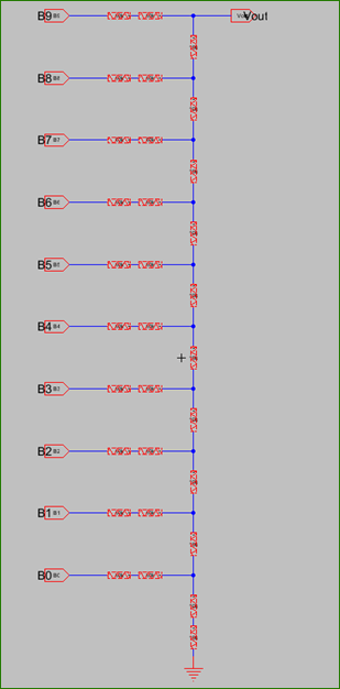
Once the circuit was laid out we need
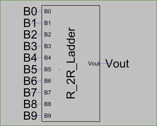
to create an icon to represent this circuit in other schematics. This was done
by creating a new icon, after exporting all the ports on the circuit. This can
be seen below.
Now that this is all done, we need to simulate the ADC_DAC circuit but with our
DAC. We start by copy pasting our DAC icon into a new copy of the ADC_DAC
simulation. We then get rid of the existing ideal DAC and wire up our own. Then
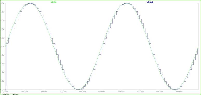
run a simulation. This simulation looks similar to the
ideal ADC_DAC output, so we know we succeeded.
Task
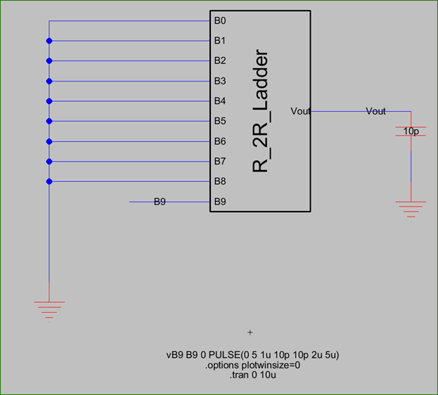
3 Test the time delay from the B9 pin when the DAC drives a 10pF load.
In order to measure time delay on the most significant
bit (MSB) we need to create a new schematic, import our DAC, and add a 10pF
capacitor to the output.
Things to be aware of:
-Be sure to extend the pins of Vout
and B9 and then label those arcs using ctrl + I. This is so spice can see these
as traces in the simulation.
-Be sure to redo the pulse command so that it inputs on B9
pin.
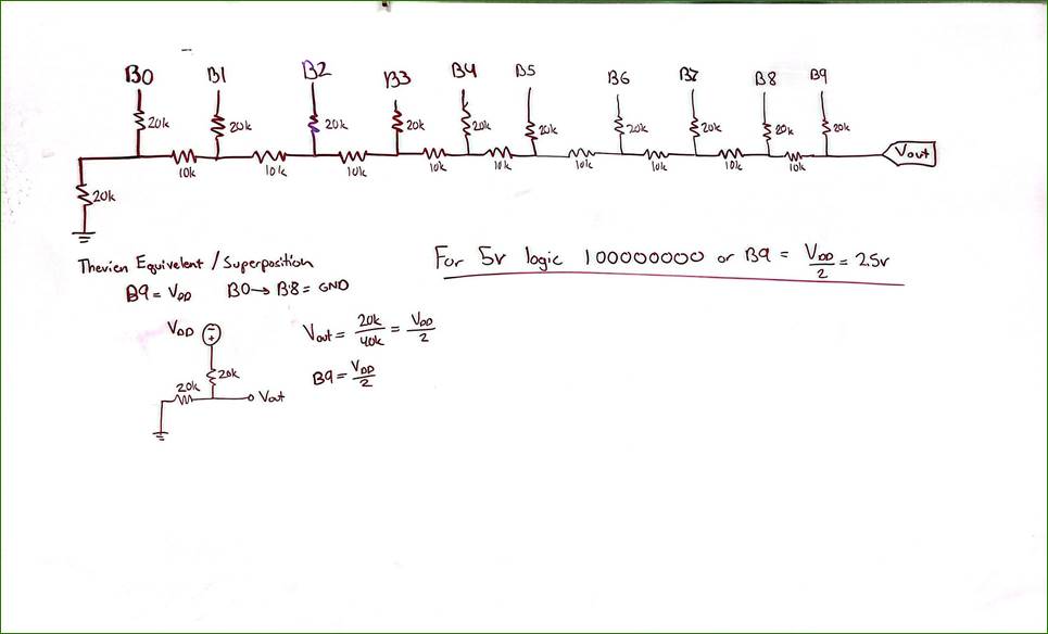
In order to get an idea of what the time delay should
be we use Thevenin Equivalent circuits and the .7RC rule to find the time delay
by hand. We can do this because this is a relatively simple circuit.
By hand the time delay is .7*10k*10pF = 70ns
Now that we’ve calculated this by hand we can simulate
using LTspice. Double click the trace to add
simulated oscilloscope traces, set these at the point where Vout
is zero and at .7 of Vout.
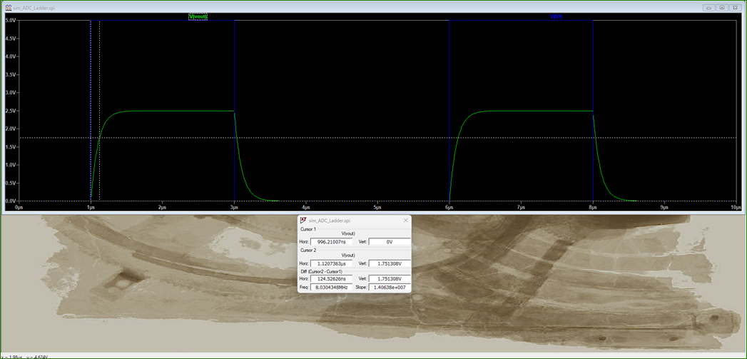
Comparing the measured time delay and calculated, I believe the measured one is
wrong because of issues simulating Vout during the
lab.