LAB 9
Building 8 bit ALU
Noah Smith
Task 1:
Design the logic circuit of the ALU. (40 points)
The First part of this process was creating
the schematic for the 8 bit ALU. This was easy enough
with the library of 8 bit gates and other devices
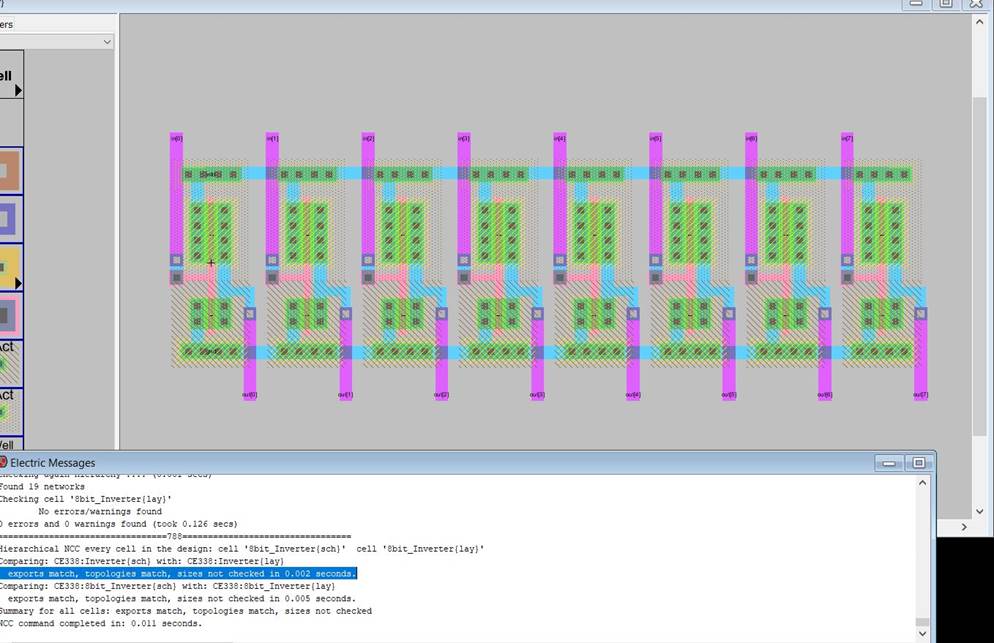
we’ve build through the semester. The only thing we were missing was an 8 bit inverter, this was a simple matter of creating a
schematic and layout using the normal inverter we already had. Pictures for the
8 bit inverter and ALU schematic can be seen below.
(DRC and NCC clean)
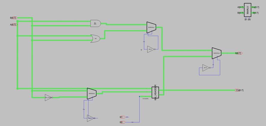
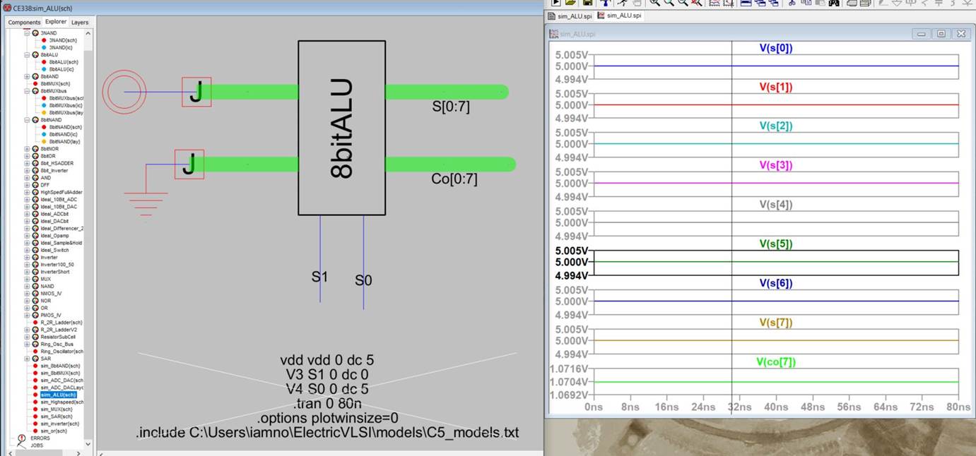
With the schematic
done for the ALU we ran a few simulations to verify the logic. It should be
able to do addition, subtraction, AND and OR logic.
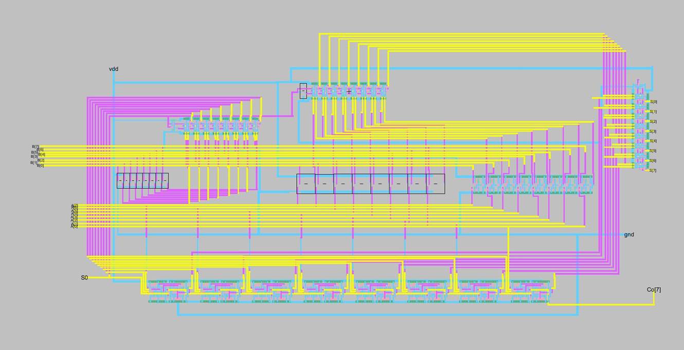
Task 2: Finish the layout of the ALU. (50 points)
With the schematic done and logic verified it
was now the “simple” matter of laying out the ALU. This starting
by importing all the individual layouts for the MUX’s Adder and AND and OR gates. Next I created the main A and B input busses.
These can be seen as the large clusters of horizontal yellow lines. Then slowly
began creating the connections from there, following the schematic. One thing
to note is that each S -> S0 loop of the MUX’s needs a single inverter.
These were added. Making sure to check DRC after every
connection and NCC at the end. Layout passes both