LAB 8
Noah Smith
Task 1:
Build an 8-bit MUX. (20 points)
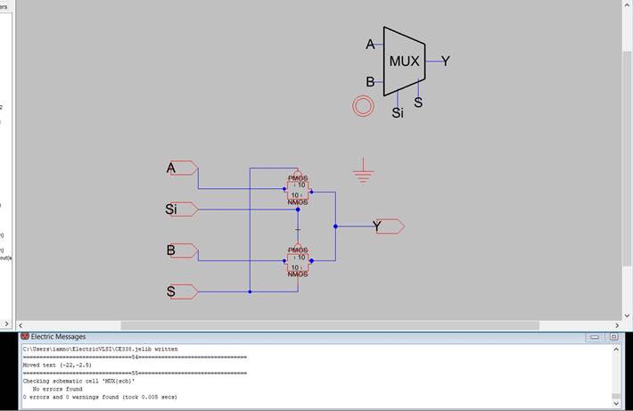
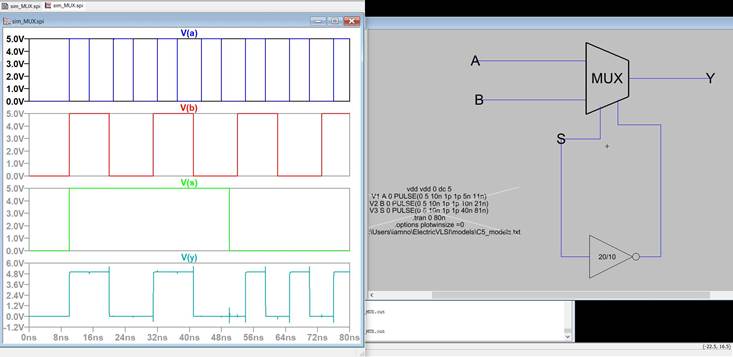
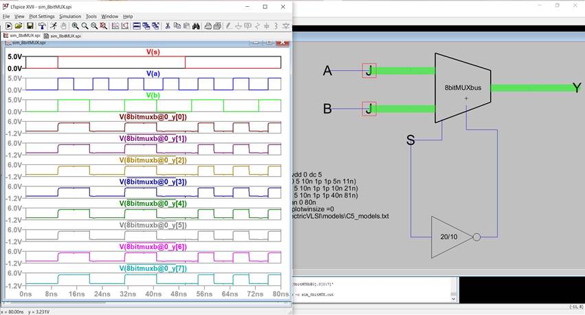
The first step was to build a single bit MUX and
simulate it using LTspice; The results can be seen
below. (Schematic is DRC clean)
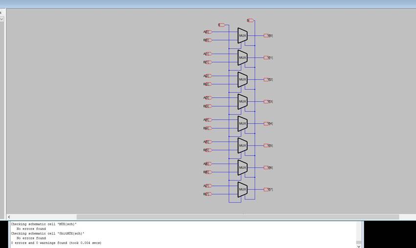
Next was the simple matter of converting this 1 bit MUX into an 8 bit MUX. The schematic and simulation of
this 8 bit MUX can be seen below.
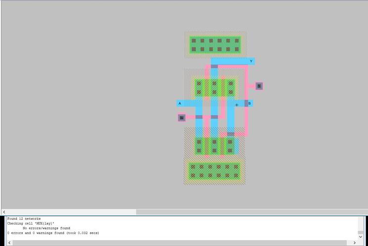
Onto the layout portion of the MUX, again
starting with the 1 bit MUX layout. This was laid out
in a way to be easily chained together into an 8 bit
layout with minimal tweaks or complications. (DRC and NCC are clean for this
layout)
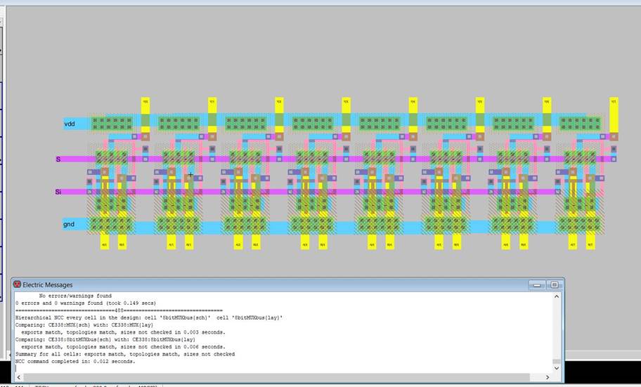
As mentioned previously the next step is to get
8 of this mux’s in a line and wire it up (8 bit MUX).
This passed both DRC and NCC checks.
Task 2:
Build a 1-bit high-speed full adder. (40 points)
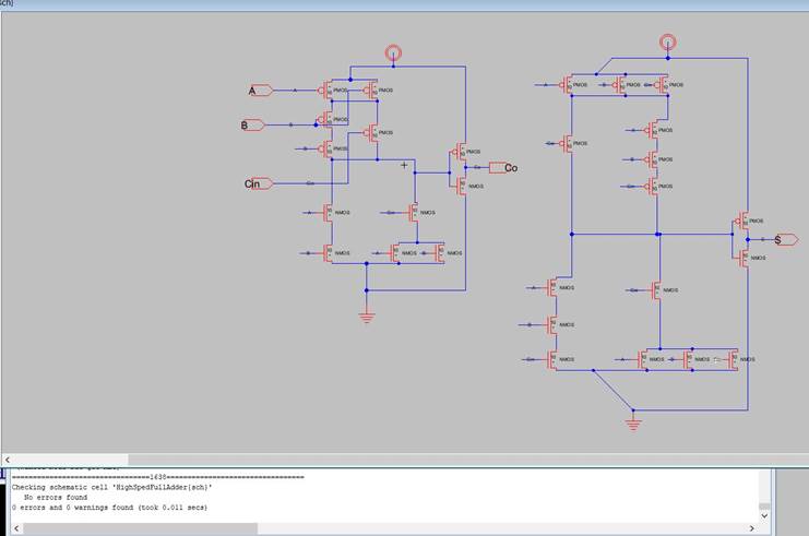
To start creating a high
speed full adder I used the AOI logic schematic to create a layout. Then
built the schematic in Electric VLSI and simulated using LTSpice.
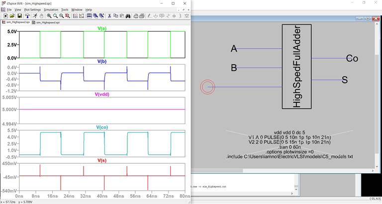
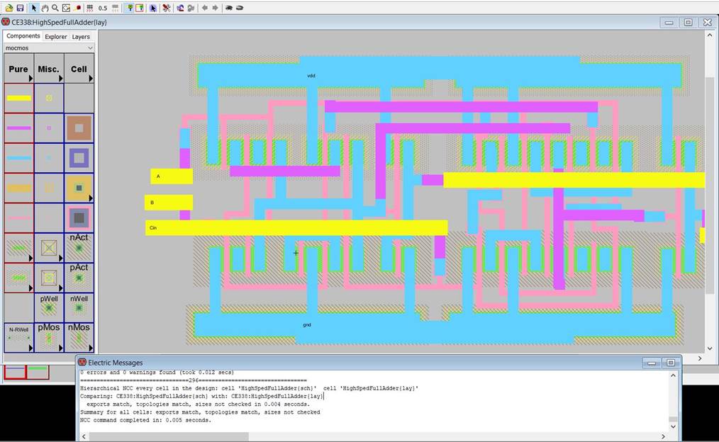
With the schematic done it was a slow process
of carefully laying out this high speed FA in a space
efficient way. It takes inspiration from the layout pictured in the tutorial
makes “improvements” when I saw a better way to do something. (passes DRC and
NCC)
Task 3:
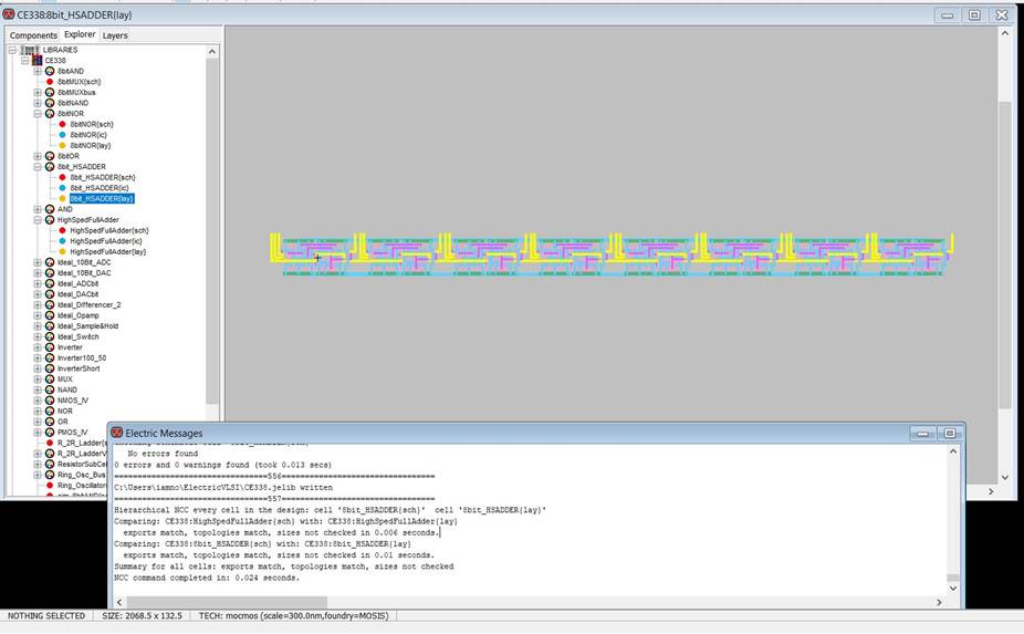
Build an 8-bit high-speed full adder. (30 points)
With the most challenging part of the layout
done, I now had to simply smoosh 8 of these together. With the layout designed
in a way to make this simpler it was a fairly straight
forward process. Again, started with the schematic and simulation.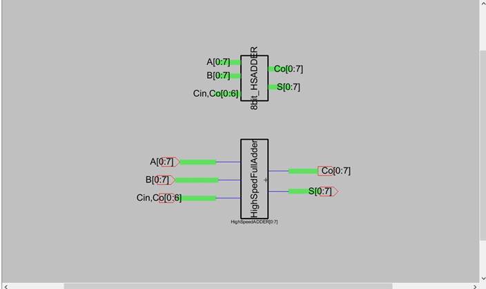
Onto the layout, not a lot of detail in this
image but all pins are exported correctly and it
passes NCC and DRC.