LAB 7
Noah Smith
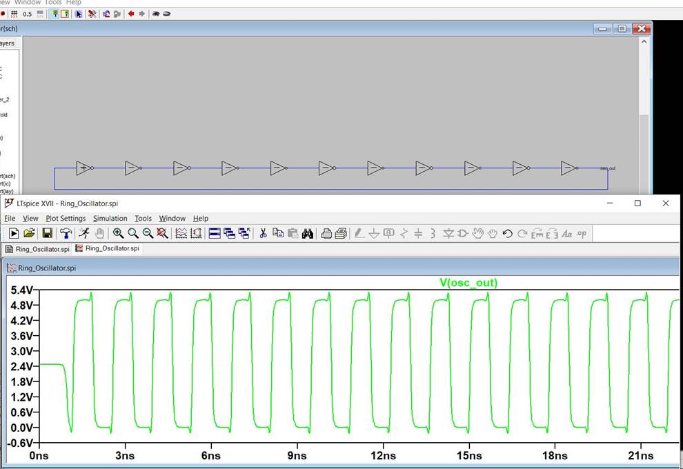
Task 1: Build and simulate a Ring oscillator. (20
points)
After breifly modifying my
existing inverter design, I could design the schematic for the Ring oscillator
by chaining 11 inverters together. A simultation was run to ensure proper
functionality.
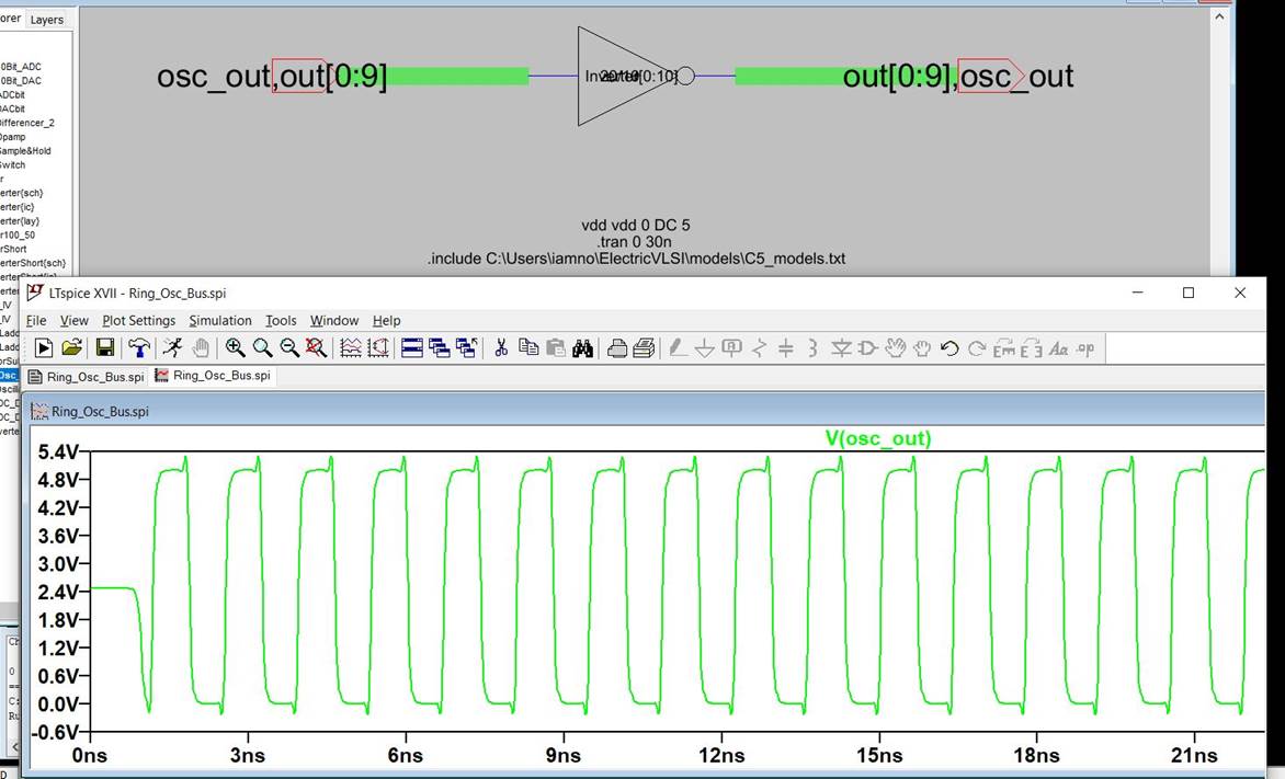
Next we created the same
schematic with buses instead of 11 different inverters, this was done by
renamin the inverter icon to inverter[0:10] and using buses to connect the
input and output ports. Again, simulated to check logic.
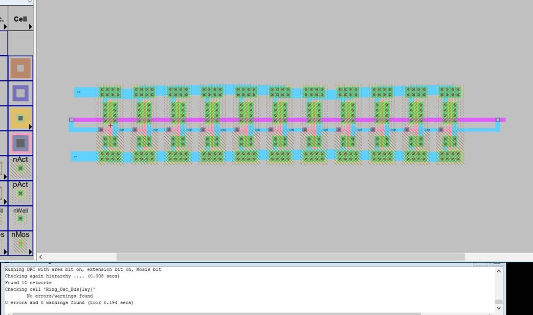
After creating the schematic with buses and
verifying logic, we could create the layout. This was simple enough, line 11
inverters in a row, connect vdd’s and gnd’s link all the in’s to the outs and
short the final in and out together with metal 2 layer (purple). Verify that it
is clean (Clears NCC and DRC).
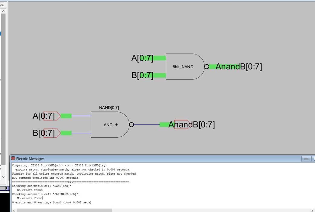
Task 2: Design an 8-bit AND gate. (20
points)
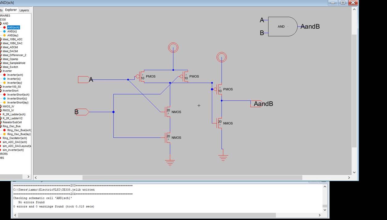
Using our new bus knowledge we can create an 8
bit AND gate. First we need to create an AND gate by tossing an inverter on the
output of our NAND gate schematic. DRC check was clean.
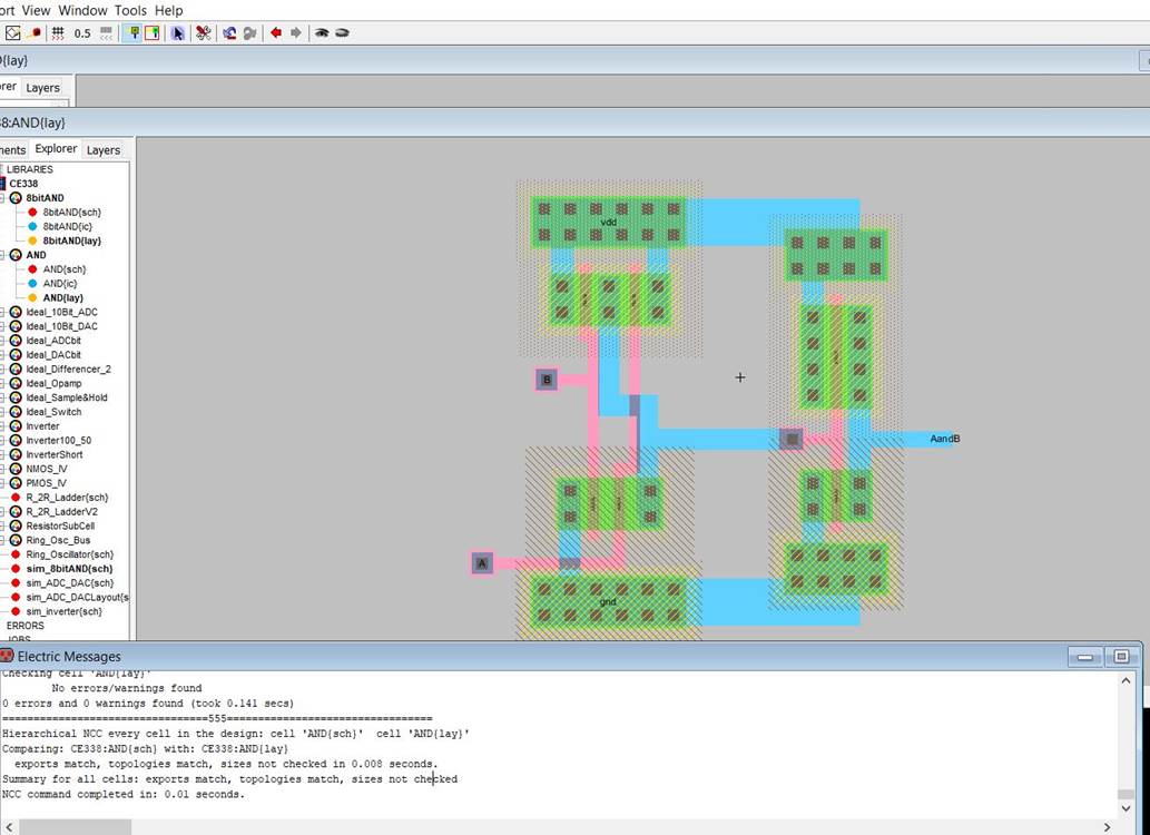
Next to create the layout of this AND gate.
Again, take an inverter and plug it into the output of our NAND layout. Ensure
it passes NCC and DRC.
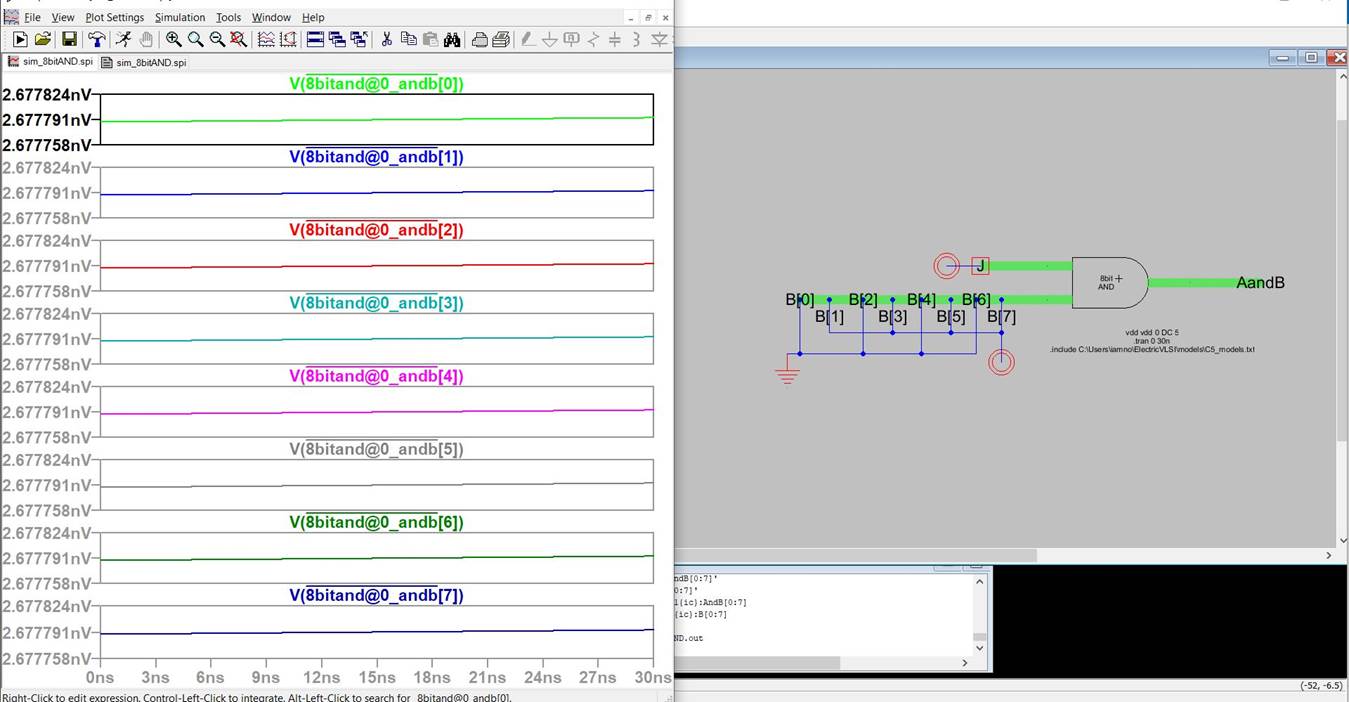
Next using the icon of the AND gate, rename it
to AND[0:7] to create an 8 bit and gate, wire up 8 different inputs with buses
and name your outputs accordingly. Run a quick
simulation to check logic.
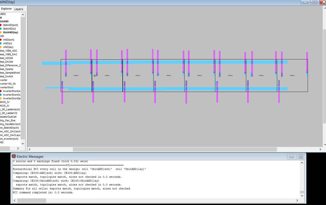
Now simply line the AND gate
layouts in a line, connect the things that need connecting, export the pins and
boom 8 bit adder. Make sure it clears NCC and DRC.
Task 3: Design an 8-bit OR gate. (20 points)
Now that we’ve created an 8 bit AND gate we
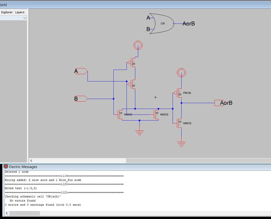
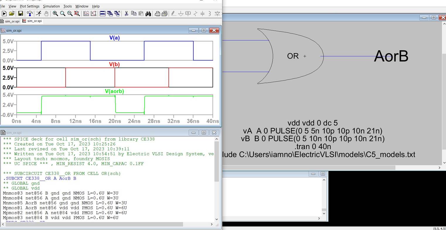
will do the same with an OR gate. First step is to create a single bit OR gate.
This is done like before, by chucking an inverter on the output of our existing
NOR gate schematic. Ensure it passes DRC and then run a quick simulation.
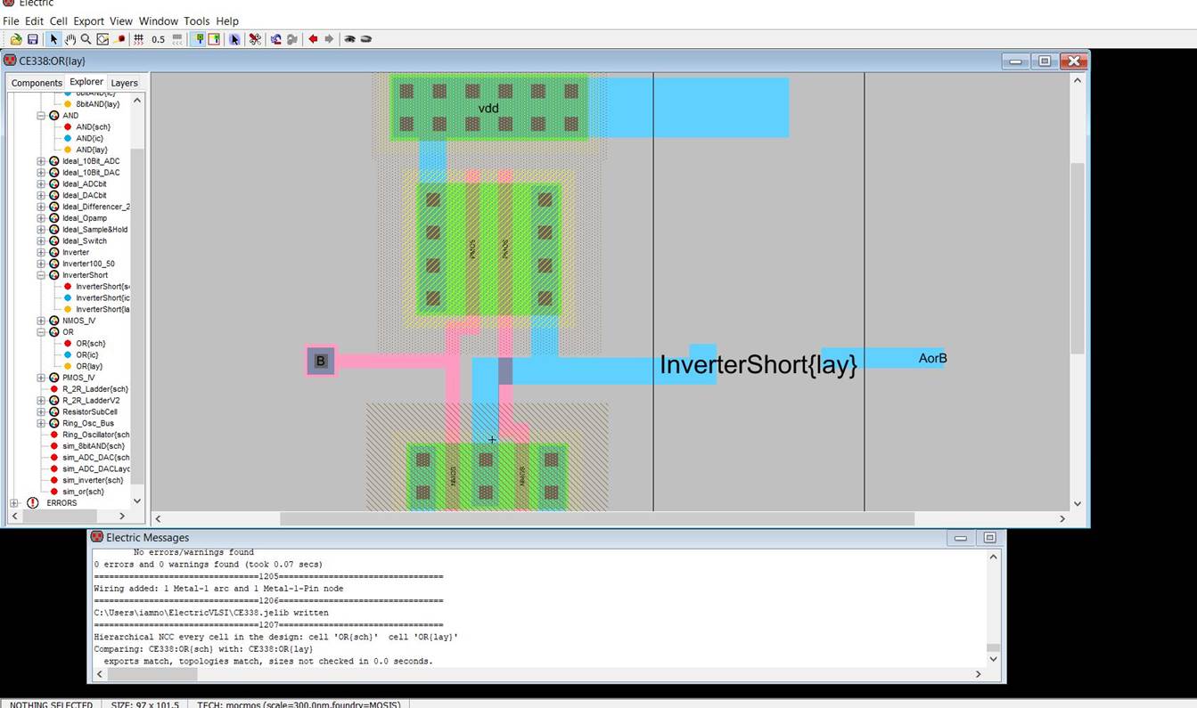
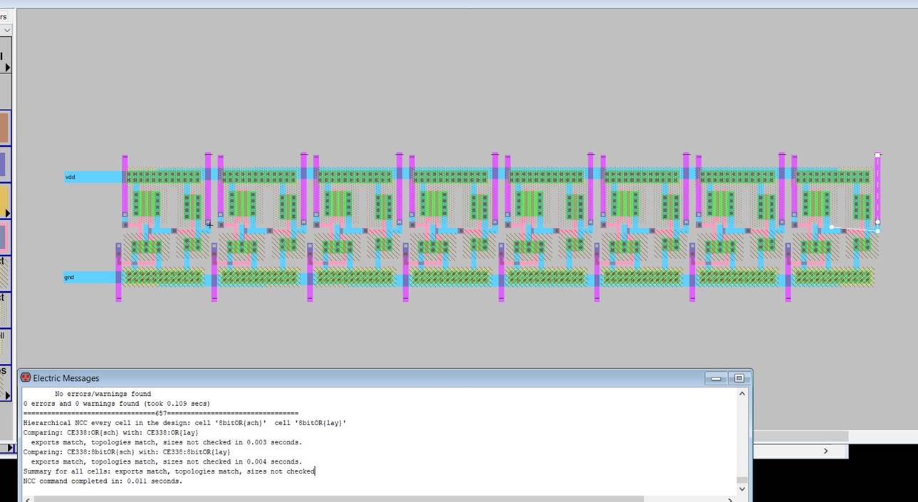
Now create the layout view of
the OR gate. Import the inverter layout and hook up gnd, vdd and export the
apropreate pins.
Chain 8 of the OR gate layout together, connect
vdd, gnd and use Metal 2 to get the export pins beyond the rails. Export all appropriate
pins. Check NCC and DRC.
Task 4: Design an 8-bit NAND gate. (20
points)
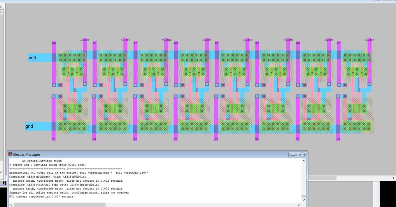
To build an 8 bit NAND gate, follow the exact
same process as the previous 2 gates. Create a schematic for the NAND logic
then create the layout from there. Ensure it passes DRC and NCC at this stage.
Next chain 8 of these gates together, use metal 2 to get the export pins out of
the rails, wire vdd and gnd together and run DRC and NCC. Tip: make sure the layout
of the NAND gate passes NCC with the NAND gate before making it an 8 bit
layout. This will save many headaches.
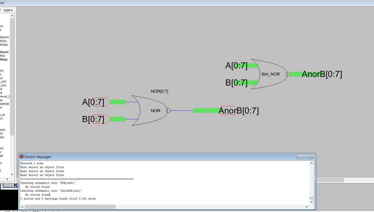
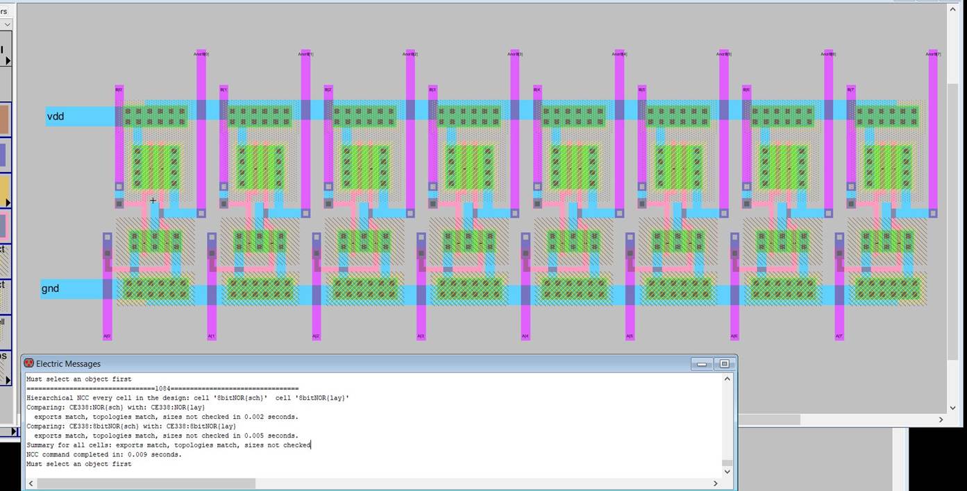
Task 5: Design an 8-bit NOR gate. (10
points)
Same process as the previous 3 steps, but now with
NOR logic. Use existing NOR gate to create 8 bit schematic, check NCC and DRC
on the single NOR gate before combining and then combine into the 8 bit
schematic. Connect vdd and gnd. Export appropriate pins. Run NCC and DRC.