LAB 6
Noah Smith
Task 1: Create the schematic and layout of the
NAND gate. (15 points)\
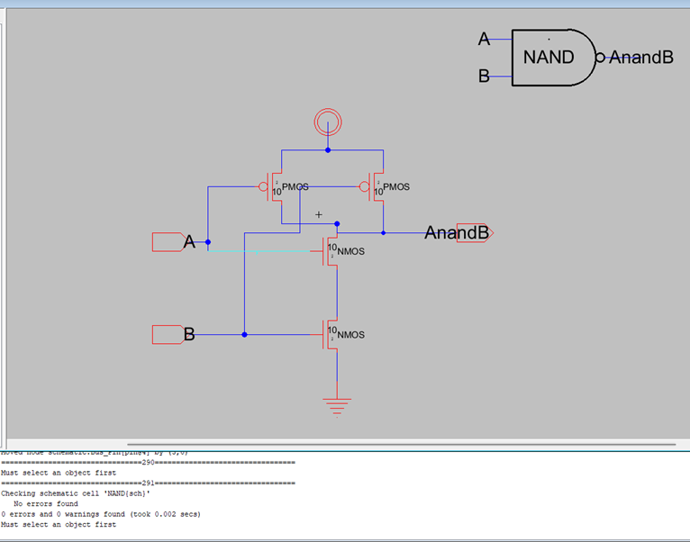
Creating the schematic
of the NAND gate logic using NMOS and PMOS transistors as well as an icon view,
DRC was clean.
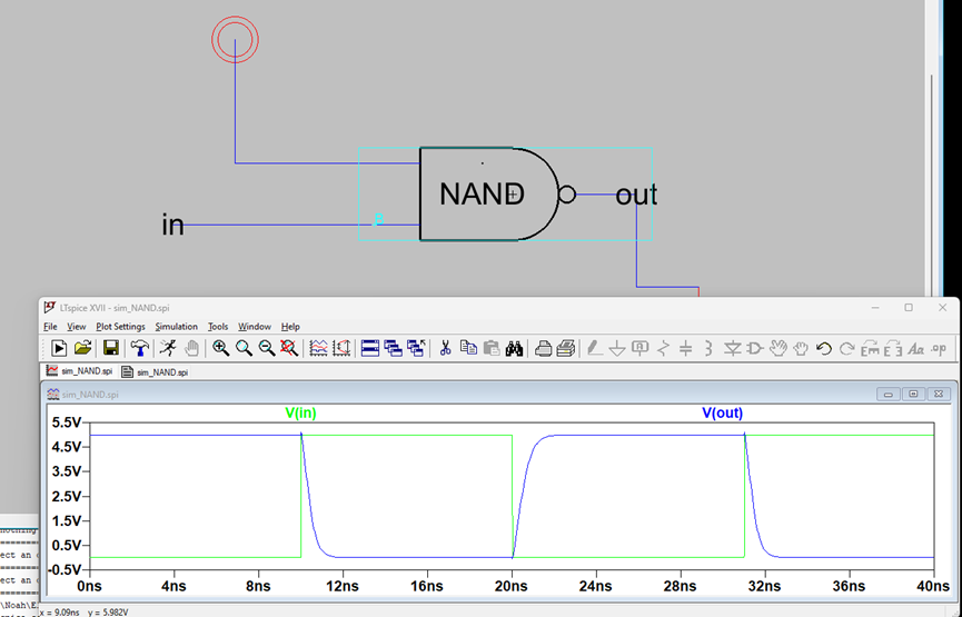
Working
simulation of NAND gate simulated with LTspice.
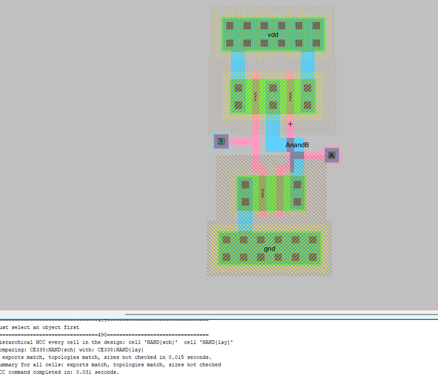
Creating
the layout view and making sure it passes NCC check.
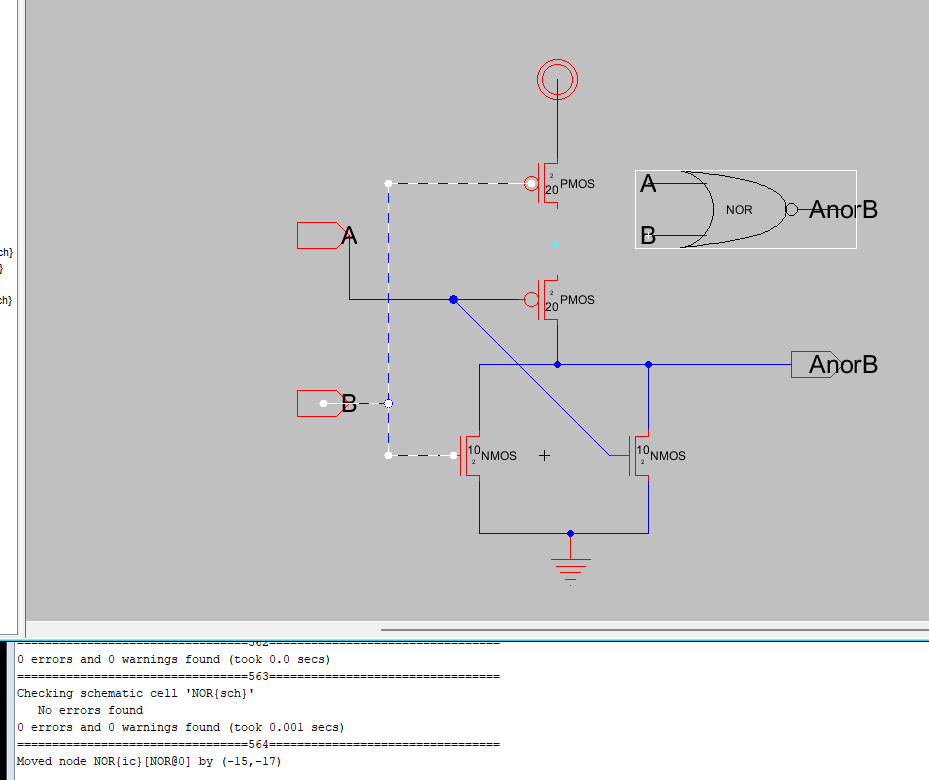
Task 2: Create the schematic and layout of the
NOR gate. (15 points)
Creating schematic for NOR gate using NMOS and PMOS
transistors, Passes DRC.
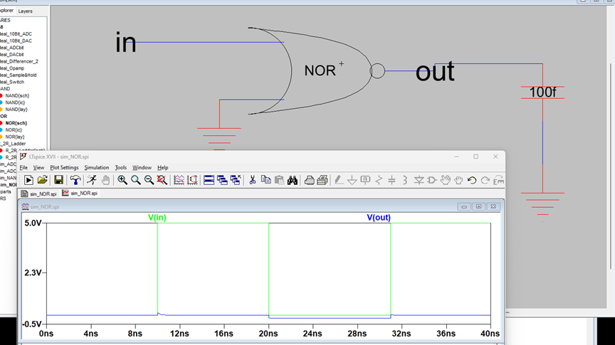
Simulating
NOR gate using LTspice.
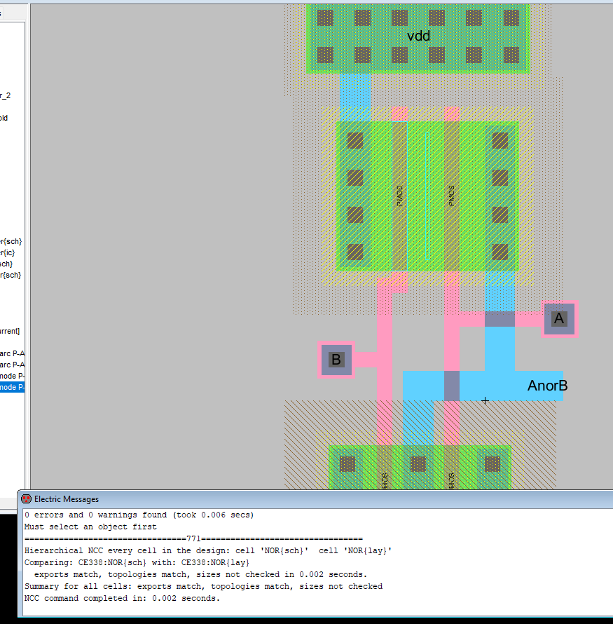
Creating
layout of NOR gate, passes NCC.
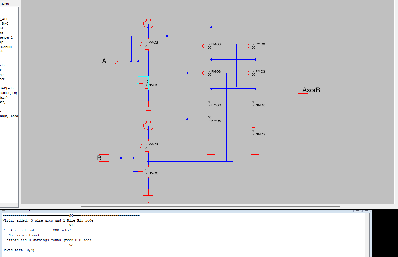
Task 3: Design, simulate, and layout an XOR
gate. (30 points)
Schematic of XOR gate
passes DRC.
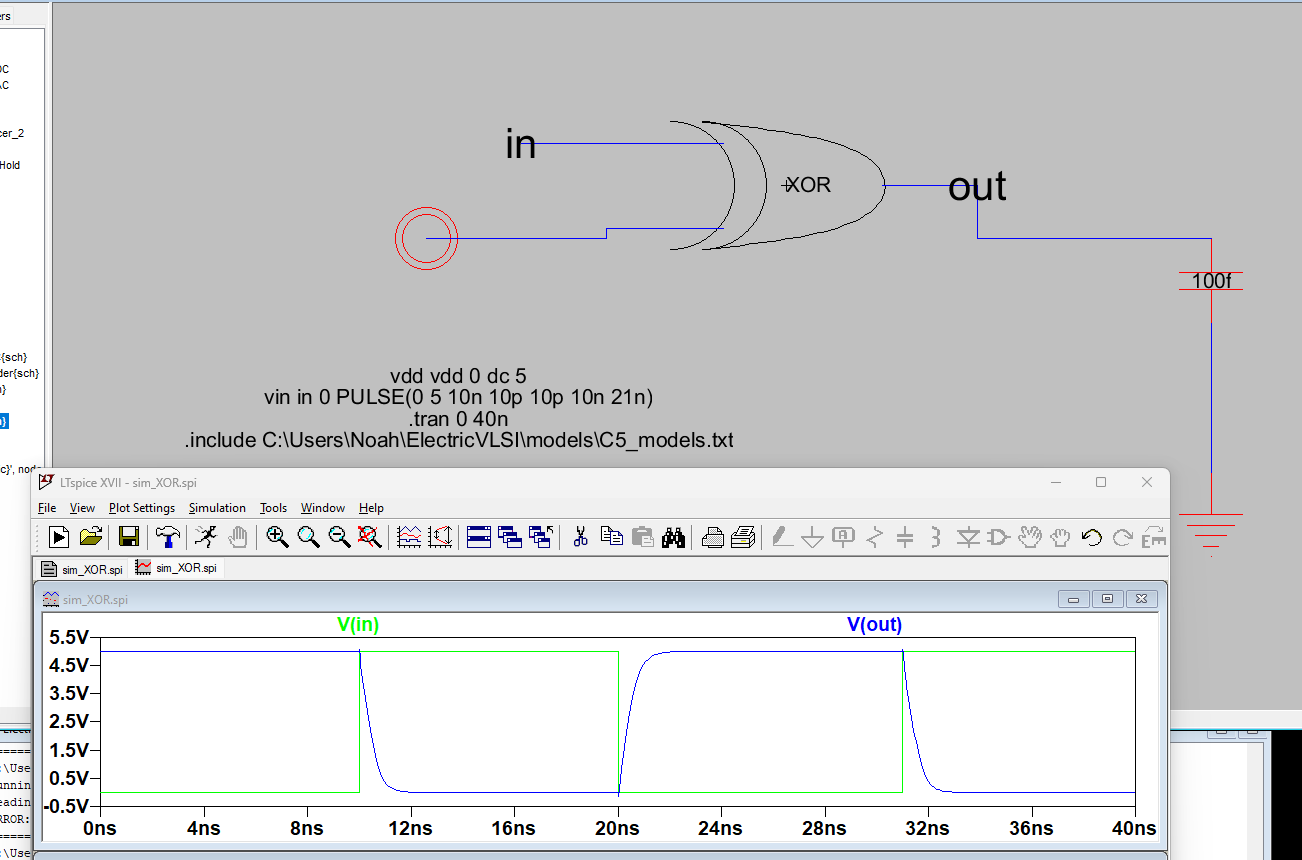
Simulation of XOR gate
using LTspice.
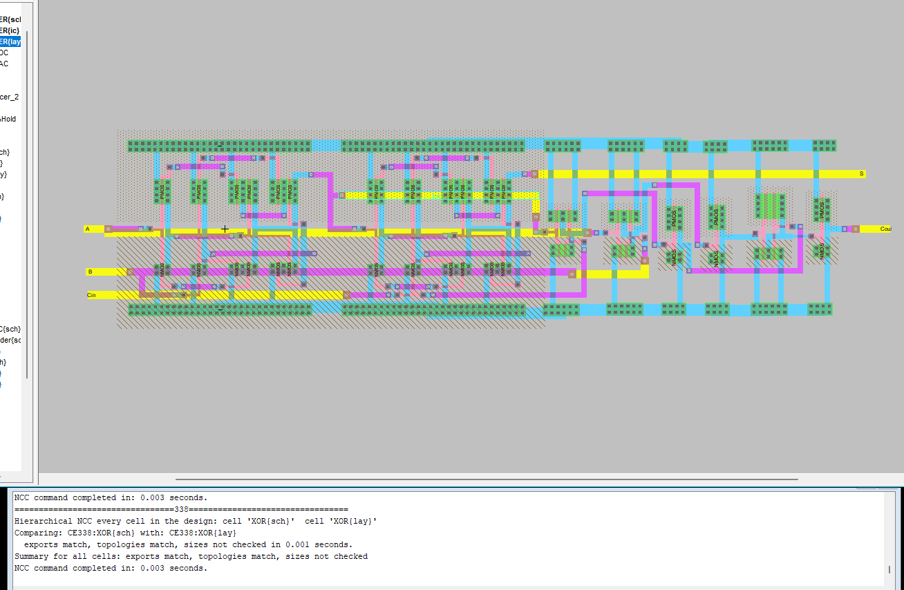
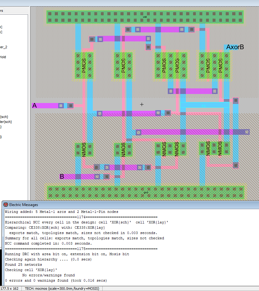
XOR Gate layout passes
NCC.
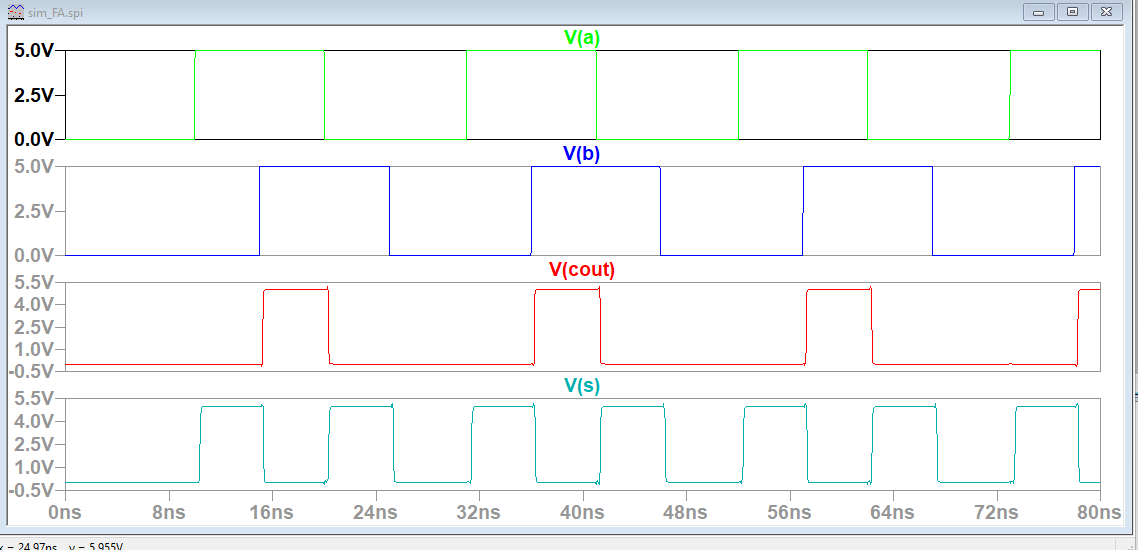
Task 4: Design, simulate, and layout an Full Adder. (30 points)
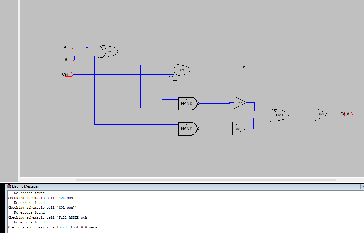
Schematic and gate logic
for Full adder. Passes DRC.
Full Adder simulation with
Cin connected to Gnd
L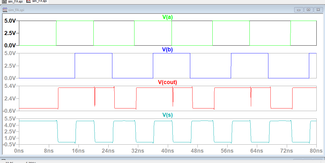
Simulation of Full adder
with Cin connected to Vdd (5V)
Layout of Full Adder
using all 3 metal layers present in C5 technology. Leads are all in metal 3