LAB 2:
BASIC LOGIC GATES
Noah
Smith
Tasks 1 &
2:
1.
Go through all the steps in this lab instruction, report your code,
simulation results, and the on-board verification results. (30 points)
2.
Use the same procedure to create XOR and OR gates. Run simulations to verify the
logic. (30 points)
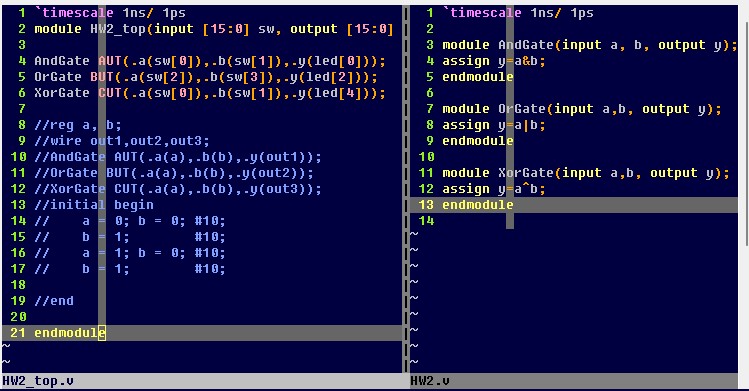
I did tasks 1 and 2 simultaneously. I created one .v file with all 3 logic gates in their own modules as seen below. I then combined all these in the same test bench. There is a slight error in the screen shot captured here as the SW ports tied to the XOR gate were not correctly remapped after copying and pasting the lines down. This was fixed for the upload to the board. The commented-out lines of code are the code used for the test bench, again all 3 gates done simultaneously, with different outputs
.
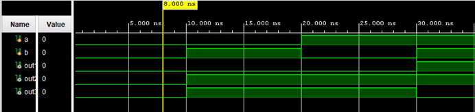
Below are the simulation results of simultaneously simulating
all 3 gates.
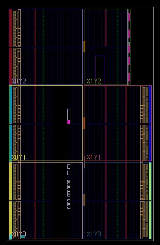
Finaly a picture of the implementation process of this board.
This is only for the AND gate as it was what I ran as a sample for the full
process.
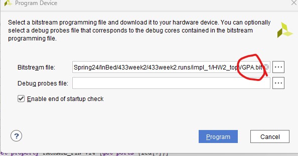
Below is a video of all these gates working on the same program (Programed using QSPI).
3. Use both the volatile and nonvolatile methods (QSPI) to program your FPGA. Show videos for the demonstrations. (40 points)
This task was done the video above was programed using the .bin file and and the device in QSPI mode, and then the memory cleared and the device reporgamed using the .bit file and in JTAG mode.