ENGR338 Lab 2022
Fall
Lab 8
MUX and Full Speed Adder
Name: Mason
Brady
Email:
mrbrady1@fortlewis.edu
MUX and High Speed FA
Introduction:
This lab uses Electric VLSI and LTSpice to simulate pmos and nmos gates
in order to create a MUX, 8-bit MUX, a High Speed Full Adder, and an
8-bit High Speed Full Adder.
Materials:
LTSpice, Electric VLSI
Methods:
First, a 1-bit MUX was created in Electric. The VDD and GND were added
to appease LTSpice. The Icon was then created for the schematic as seen
below in Figure 1.
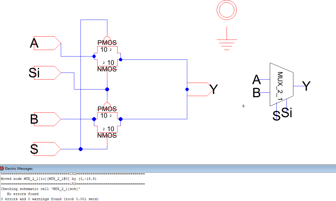
Figure 1.
MUX Schematic and Icon.
The MUX icon was then used to create an 8-bit MUX using busses. The
schematic can be seen below in Figure 2.
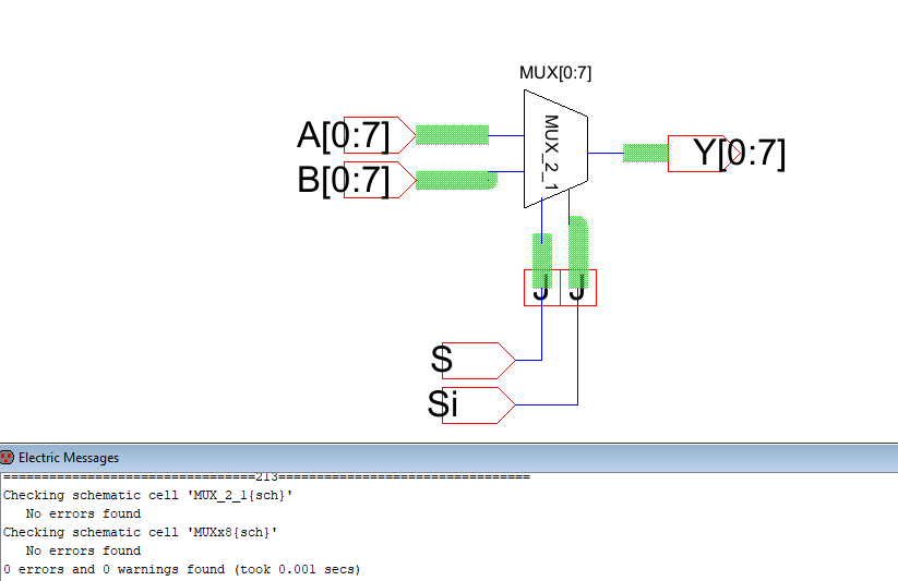
Figure 2. 8-Bit MUX
Schematic with busses
A
layout was then created which for the 1-bit was pretty straight forward.

Figure 3. 1-bit
MUX layout.
The 1-bit MUX layout was then arrayed to create 8 identical layouts and
the MUXs were then wired together to create the following layout.
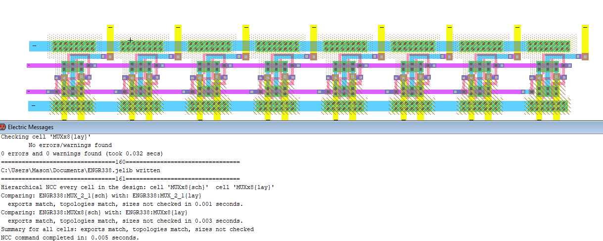
Figure 4. 8-bit MUX
layout.
All of these layouts and schematics were pretty straight forward and
easy. After the completion of the MUX the high speed full adder was
created.
The schematic for the high speed full adder can be seen below, the
logic for the circuit was provided and made this task much easier. The
schematic and icon can be seen below in Figure 5.
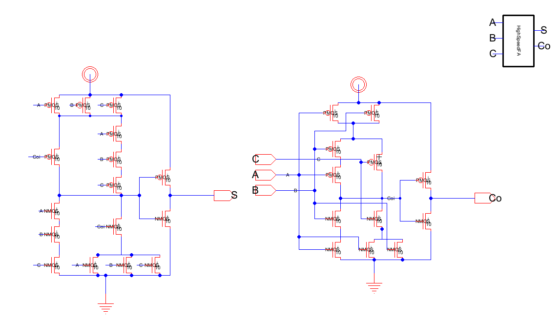
Figure 5. High
Speed Full Added schematic
The full adder was then laid out. I opted for what I thought was a
simpler layout for the summing block then the sample layout. I used
parallel gates which used the same trigger signal. I thought this made
the layout a little cleaner even if it used slightly longer poly wires.
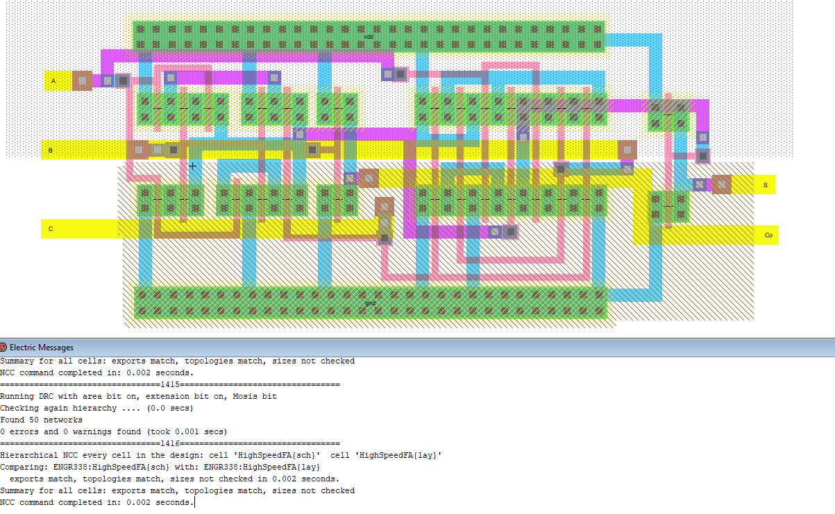
Figure 6. High
Speed Full Adder Layout.
An 8-bit version of the high speed full adder was then created using
busses and the icon was created. The only weird thing about this
schematic is that the initial FA uses Cin and the other full adders use
the Co of the previous adder. The schematic can be seen in Figure 7
below.
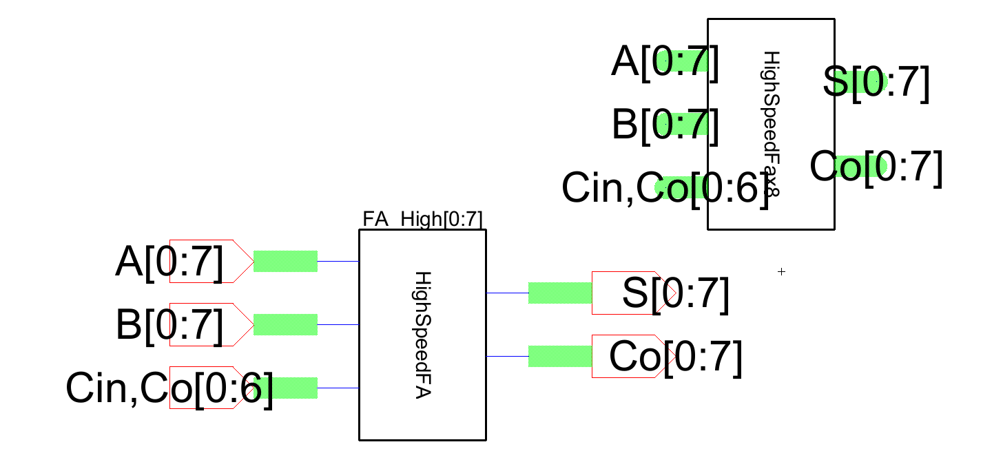
Figure 7. 8-bit
High Speed Full Adder schematic and icon.
The layout for the 1-bit full adder was then arrayed and wired together
with the previous Cout connected to the next Cin.

Figure 8.
8-bit High Speed FA layout.
Results:
The MUX, 8-bit MUX, High Speed Full adder, and 8-bit High Speed Full
Adder were all simulated and can be seen below.
First, the 1-bit MUX was simulated using the MUX and an inverter as
seen below in Figure 9.
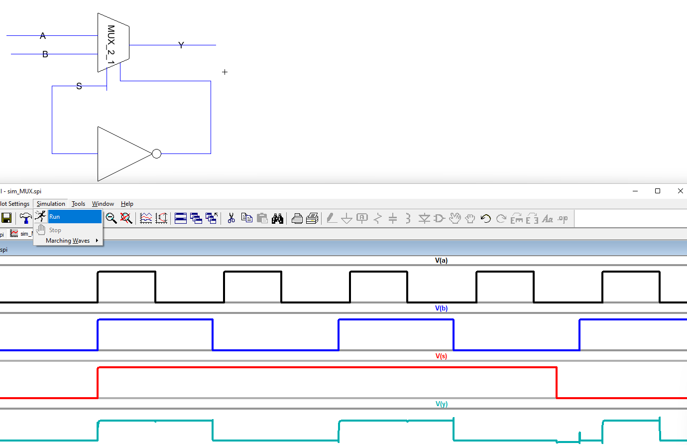
Figure 9. 1-bit
MUX simulation.
The 8-bit MUX was then simulated using a similar circuit to the 1-bit.
The outputs were all the same which was expexted since all of the
inputs were the same.
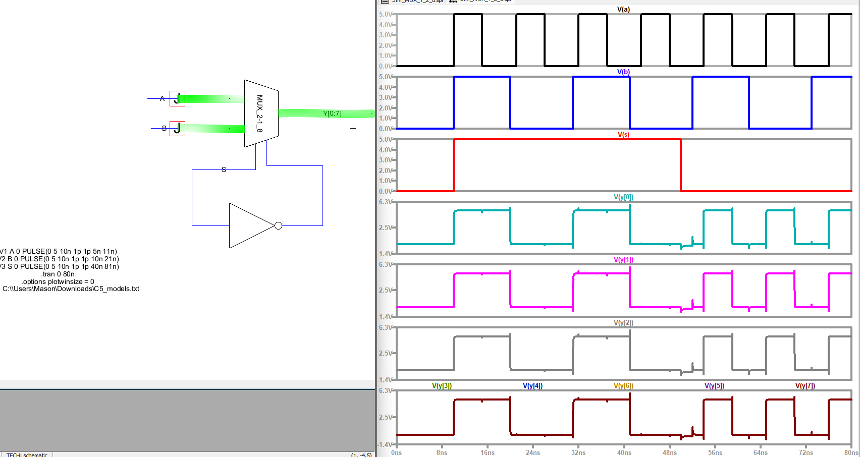
Figure 10. 8-bit
MUX simulation.
The 1-bit High Speed Full Adder was then simulated as well with the Cin
shorted to VDD so when both A and B are off the sum should be 1. The
logic checked out and the simulation can be seen below in Figure 11.
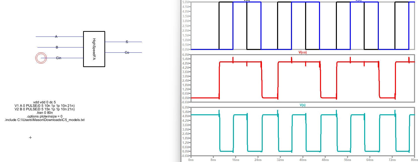
Figure 11.
High Speed Full Adder Simulation.
As per the lab instructions, the 8-bit Full Adder was simulated 3
times. The first simulation was with 11111110 and 10000000 Which should
sum to 101111110 which can be seen below in Figure 12.
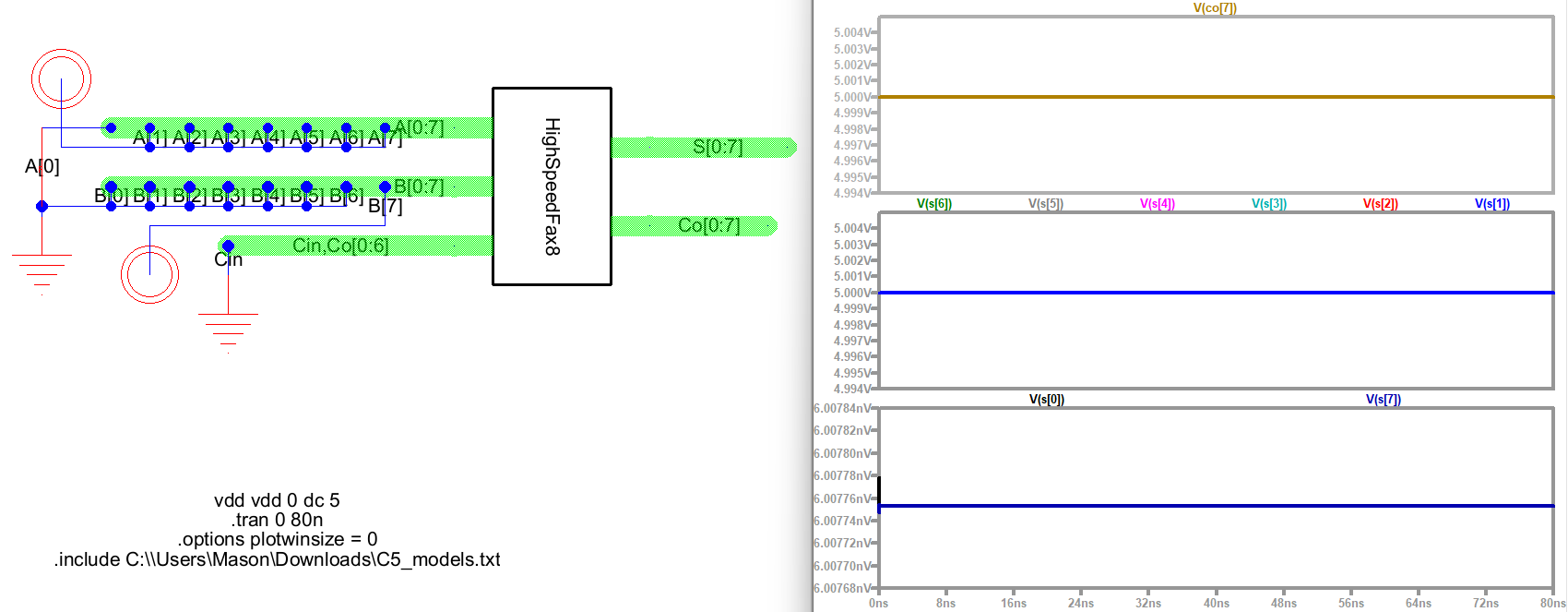
Figure 12. 8-bit
Full Adder A = 11111110, B = 10000000.
The next simulation was all zeroes to ensure that the Full Adder wasn't
picking up any weird voltages when 0 was passed. This can be seen in
Figure 13 below.
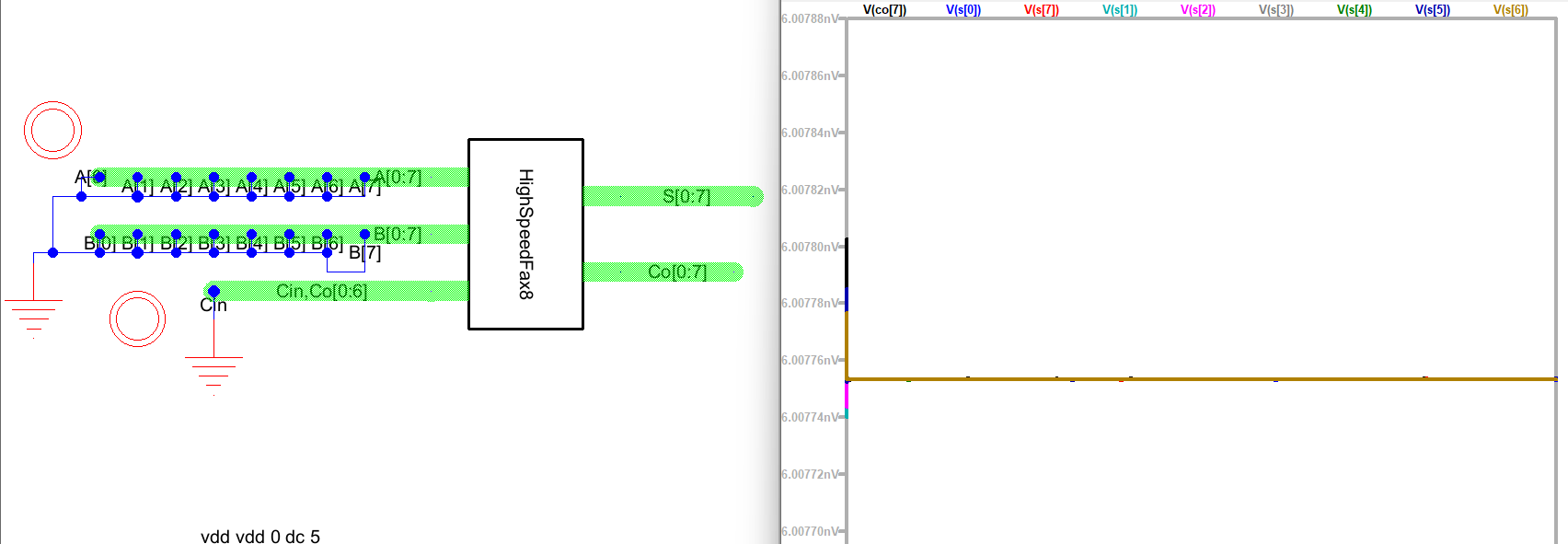
Figure 13. 8-bit
Full Adder A = 00000000, B = 00000000.
Finally, 11111111 and 00000001 were added together so the result would
be 00000000 with Co = 1 which can be seen in Figure 14 below.
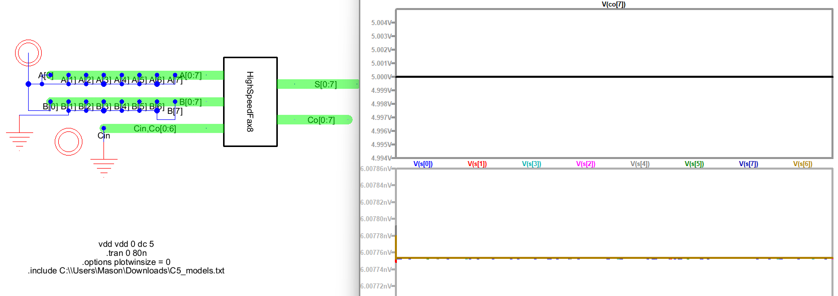
Figure 14. 8-bit
Full Adder A = 11111111, B = 00000001.
Discussion: This
lab was fairly straightforward just time intensive trying to find
enough space for vias in the FA.