ENGR338 Lab 2022
Fall
Lab 6More
gates
Name: Mason
Brady
Email:
mrbrady1@fortlewis.edu
NAND, NOR , XOR, AND FULL ADDER
Introduction:
This lab uses Electric VLSI and LTSpice to simulate pmos and nmos gates
in order to create an inverter.
Materials:
LTSpice, Electric VLSI
Methods:
First, a ring oscilator was created by putting 11 inverters in a loop.
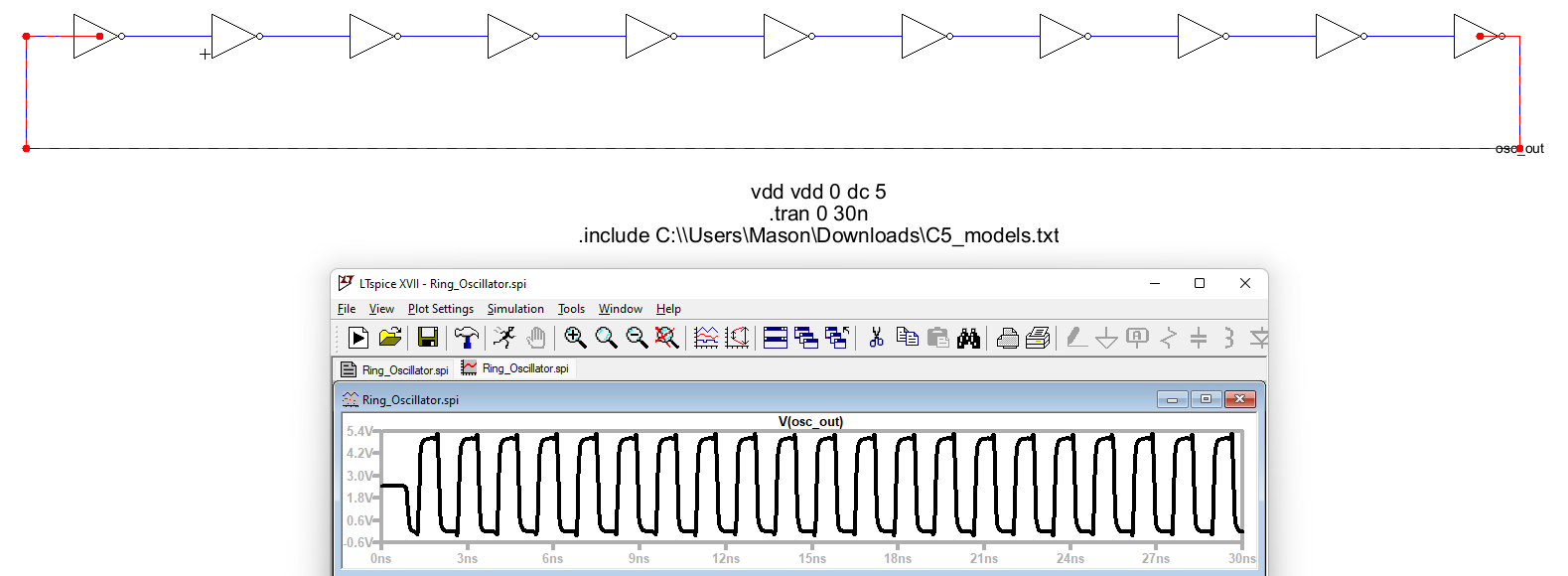
Figure 1.
Ring oscilator schematic and simulation.
The same circuit was then created using busses as seen in Figure 2.
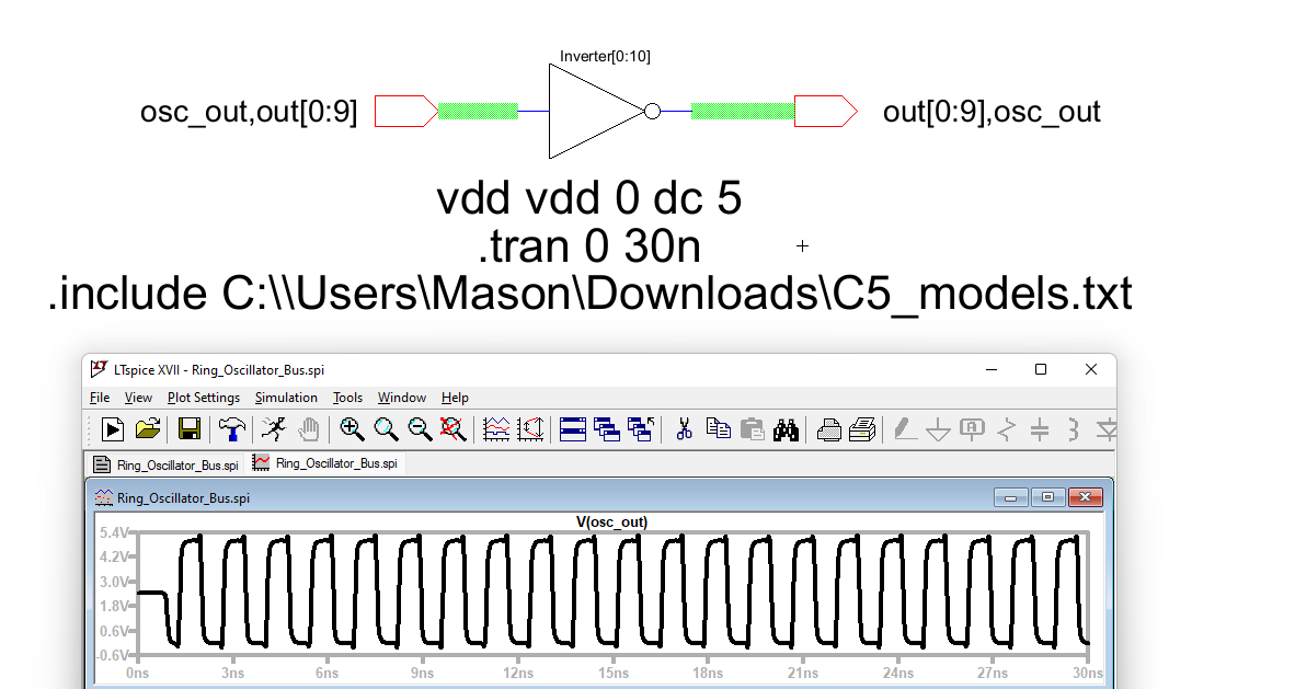
Figure 2. Ring
oscilator using busses.
The
ring oscilator was then laid out and the NCC and DRC matched and passed
as seen in Figure 3.
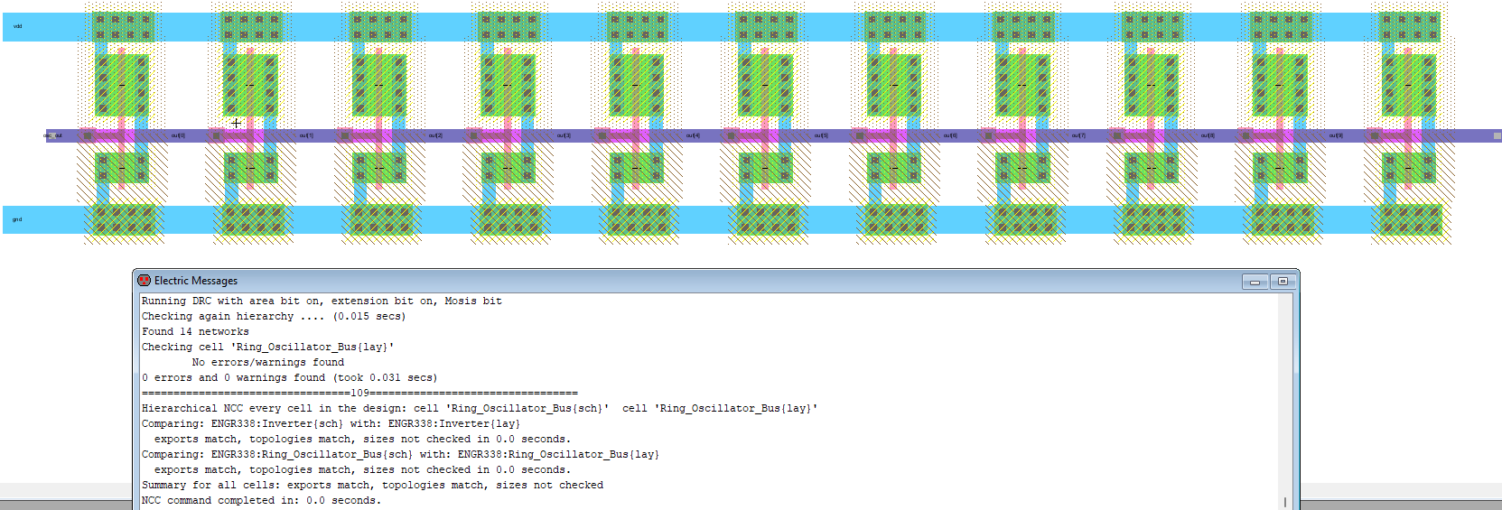
Figure 3. Ring
oscilator layout.
An 8 bit and gate was created using the same process of busees and can
be seen in Figure 4.
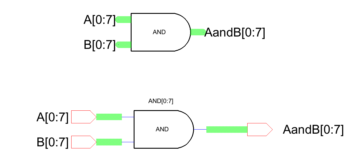
Figure 4. 8-bit and
gate schematic.
The icon was then used to simulate the 8-bit and gate.
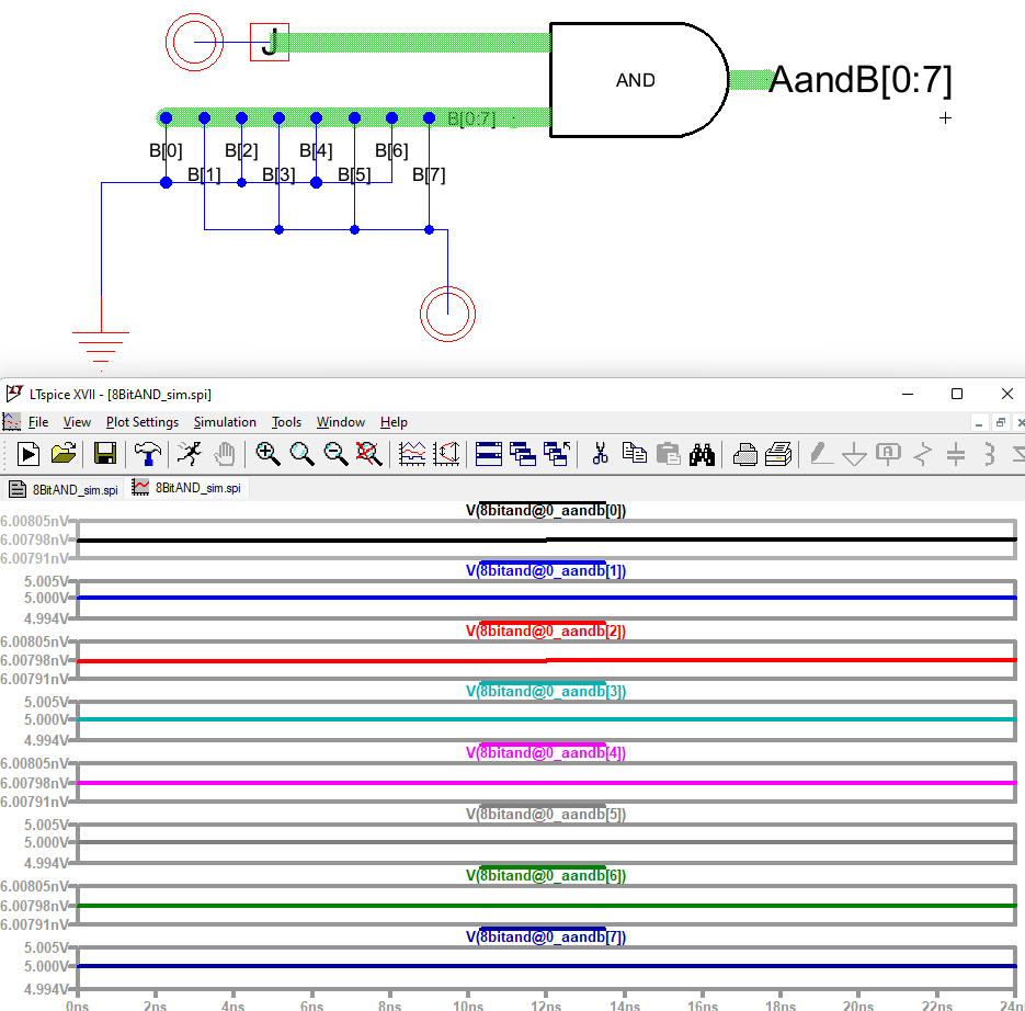
Figure 5. 8-bit and
gate simulation, even pins are grounded and odd pins are powered.
This process was repeated flipping the top pins from VDD to gnd as seen
in Figure 6.
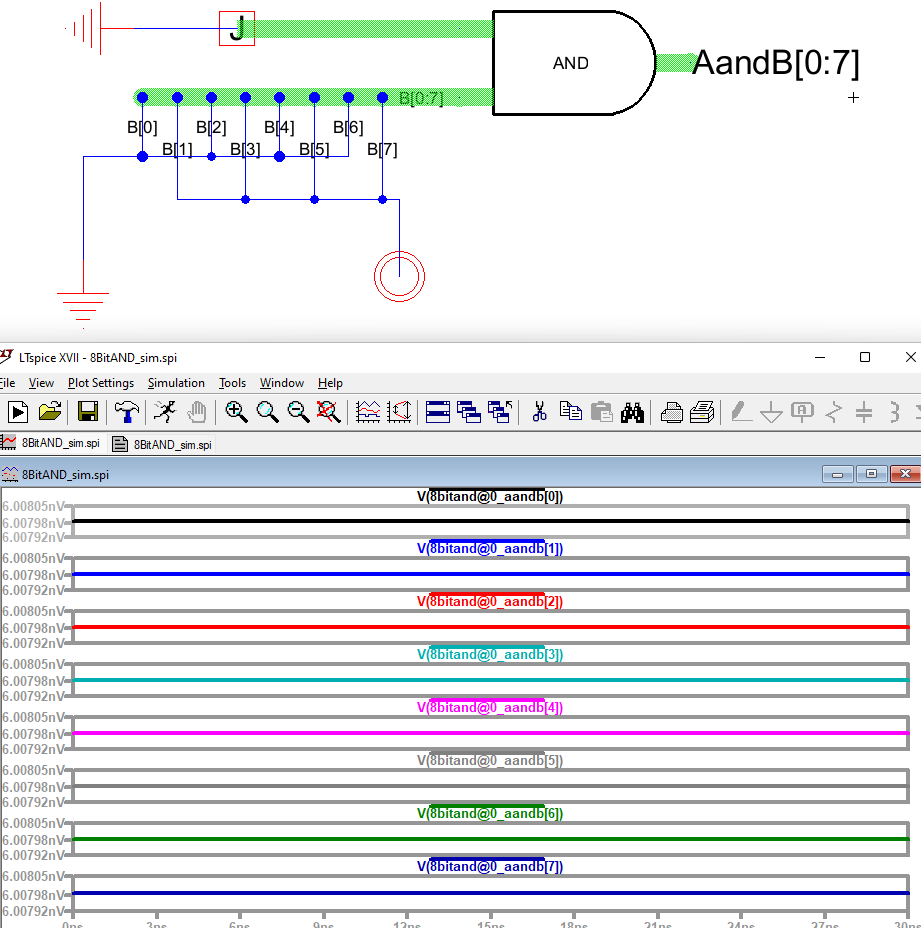
Figure 6. Simulated
8-bit and gate with top pin shorted to ground showing the logic is
right.
A layout was then created for the 8-bit and gate by copying the and
gate layout in an array and then wiring the input and outputs as seen
below in Figure 7.
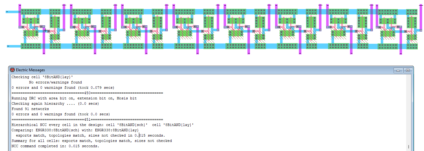
Figure 7. 8-bit
and gate layout with clean NCC and DRC.
This same process was done for an 8-bit OR gate.
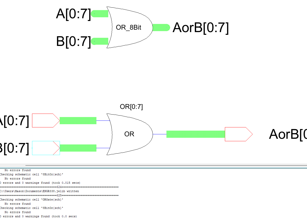
Figure 8.
8-bit OR gate using busses with no DRC errors.
The OR gate was then laid out the same way as the AND gate using an
array and then routing the inputs and outputs through metal 2.
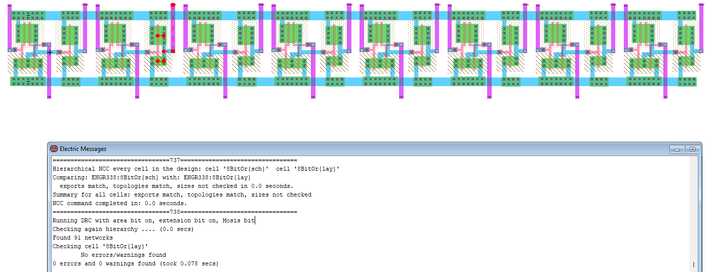
Figure 9. 8-bit
or gate laiyout with NCC and DRC check complete.
The same process was completed for NAND and NOR gates. The schematics
worked the exact same but the layouts were actually easier since they
didn't include an extra NMOS and PMOS for the inverters. The schematics
can be seen below in Figure 10.

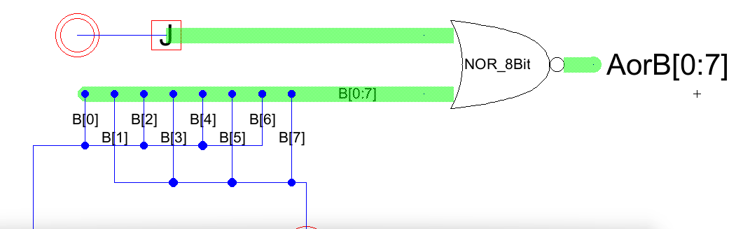
Figure 10. 8-bit
Nand and Nor gate icons created using busses the same as the And and Or
gates above.
These gates were then both simulated(in the results section) and laid
out as done earlier with the other gates. This was trivial as it was
the same as the And and Or gates just without the inverter from the
outputs. The layouts can be seen below in Figure 11.
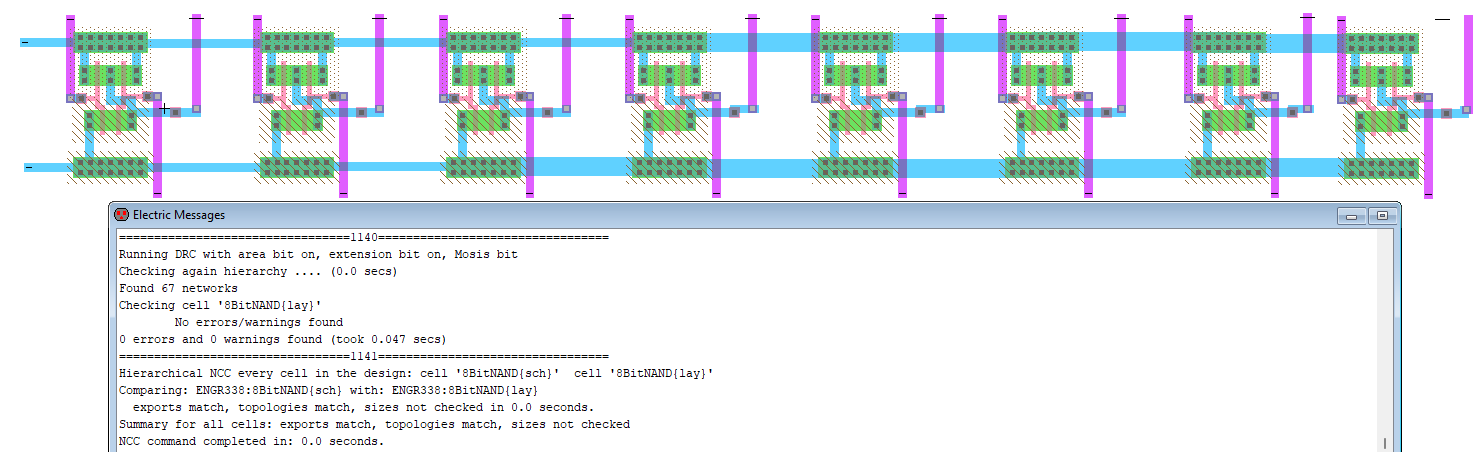
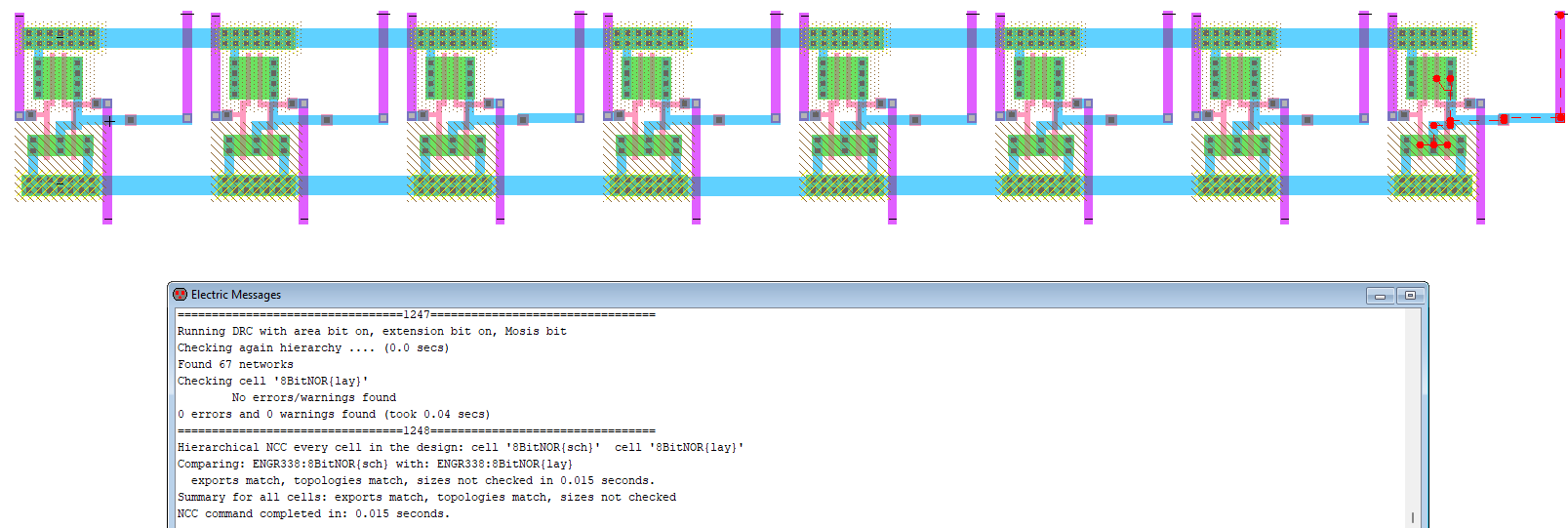
Figure 11.
8-bit NAND(top) and 8-bit NOR(bottom) layouts with clean NCC and DRC
checks.
With all of the layouts completed, the logic for the gates was tested.
Results:
The NAND, NOR, AND, OR, and Inverter gates were all known to work
before this lab so the only thing to test was if the busses were
working properly. These tests were performed by shorting the top bus to
either ground or VDD and then every other pin to VDD and the others to
ground. This test was performed with every gate except for the
oscilator.
The ring oscialtor was tested by shorting the ends together and
supplying a voltage from 0 to 5V as seen below in Figure 12.
Figure 12. Ring
oscilator simulation.
The 8-bit AND was then tested with the top pin shorted to VDD and then
the top pin shorted to GND. These tests came out with preferable
results as seen below, when the top pin was gnd all outputs were near
0V and when it was shorted to VDD the odd numbered pins output VDD as
expected.
Figure 13. 8-bit
AND gate simulation results.
The same process was completed for the 8-bit OR gate where the odd pins
should always be at voltage high while the even pins should only be
voltage high when the top bus is shorted to VDD.
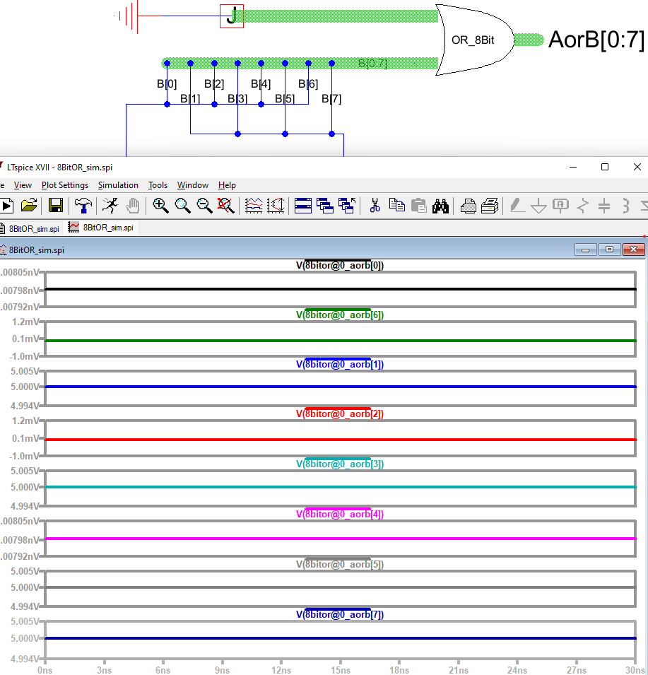
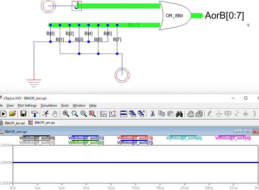
Figure 14.
8-bit OR gate simulations.
The same thing was also done for the 8-bit NAND gate where the expected
results are that the even pins should always be voltage high(will never
be 1 1) and the odd pins should only be 0 when the top bus is shorted
to VDD.
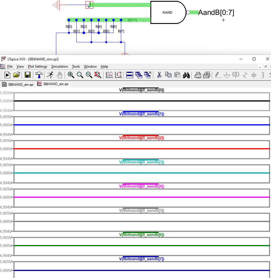
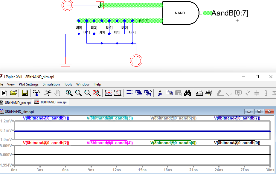
Figure 15.
8-bit NAND gate simulation.
Finally, the same thing was done with the NOR gate where the output for
the NOR gate should only be voltage high for the even pins when the top
pin is shorted to ground and all other cases should be voltage high.
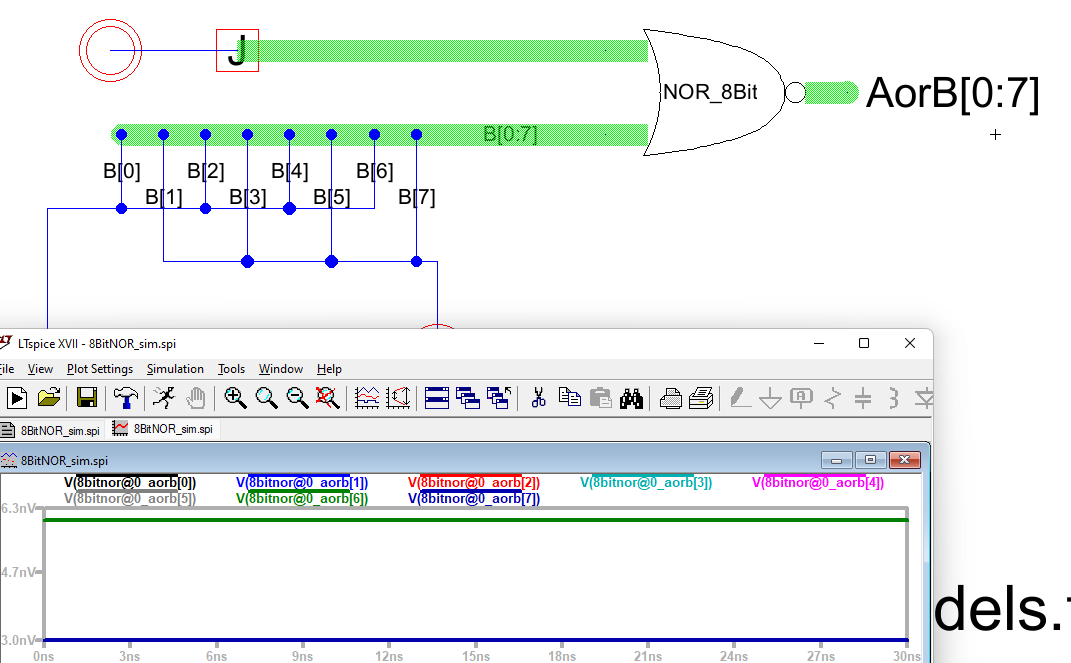
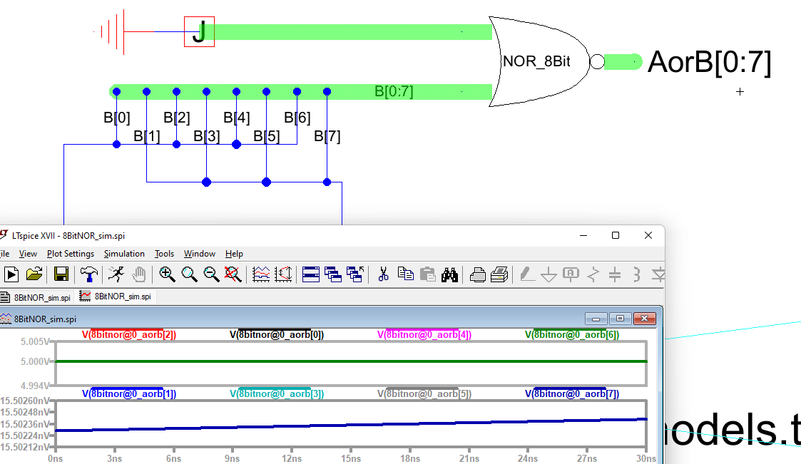
Figure 16. 8-bit NOR gate
simulation.
Discussion: This
lab was ok, it felt repetitive but no part of it was hard just a lot of
placing the same wires and running the same tests.