ENGR338 Lab 2022
Fall
Lab 6More
gates
Name: Mason
Brady
Email:
mrbrady1@fortlewis.edu
NAND, NOR , XOR, AND FULL ADDER
Introduction:
This lab uses Electric VLSI and LTSpice to simulate pmos and nmos gates
in order to create an inverter.
Materials:
LTSpice, Electric VLSI
Methods:
First, an NAND gate was created using 2 PMOS gates in parallel and 2
NMOS gates in series as seen in Figure 1 below. I am just now realizing
that I forgot to put the circle on the NAND gate so that was a mistake
but otherwise the gate functioned.
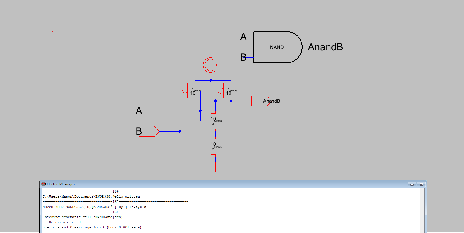
Figure 1.
NAND Schematic and Icon with 0 DRC Errors.
The circuit was then simulated in LTSpice as seen in Figure 2.
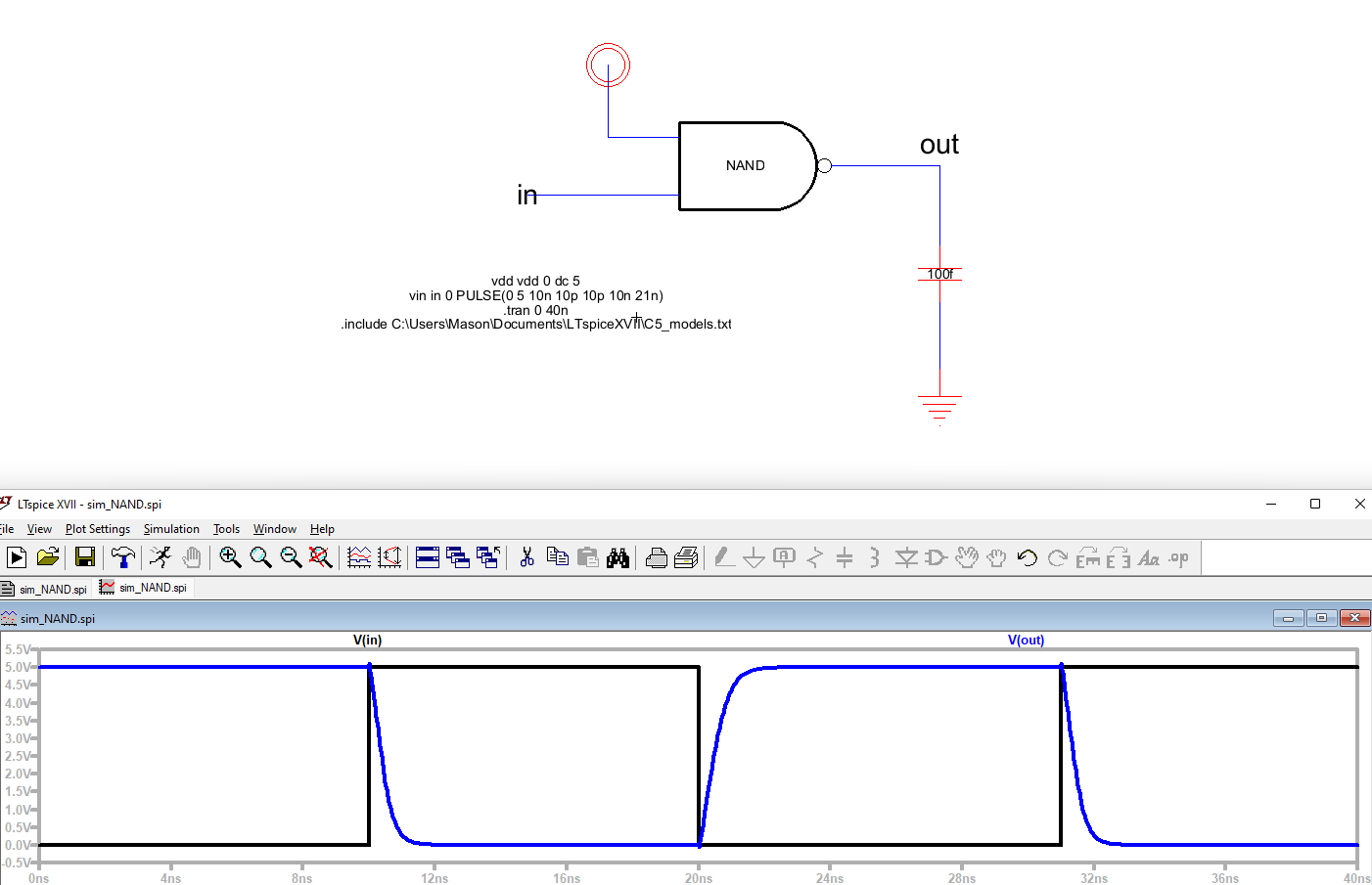
Figure 2. NAND
Simulation.
The
NAND gate layout was then completed fairly easily and passed the NCC
check and DRC with 0 errors which can be seen in figure 3.
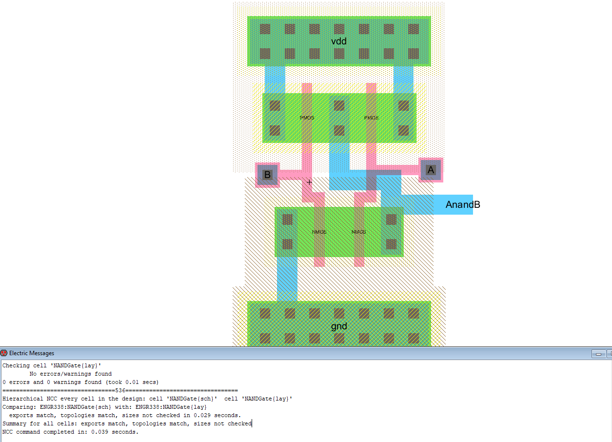
Figure 3. NAND
Gate layout.
The same process was then used for the NOR gate. The schematic can be
seen below in Figure 4. The Layout can be seen in Figure 5.
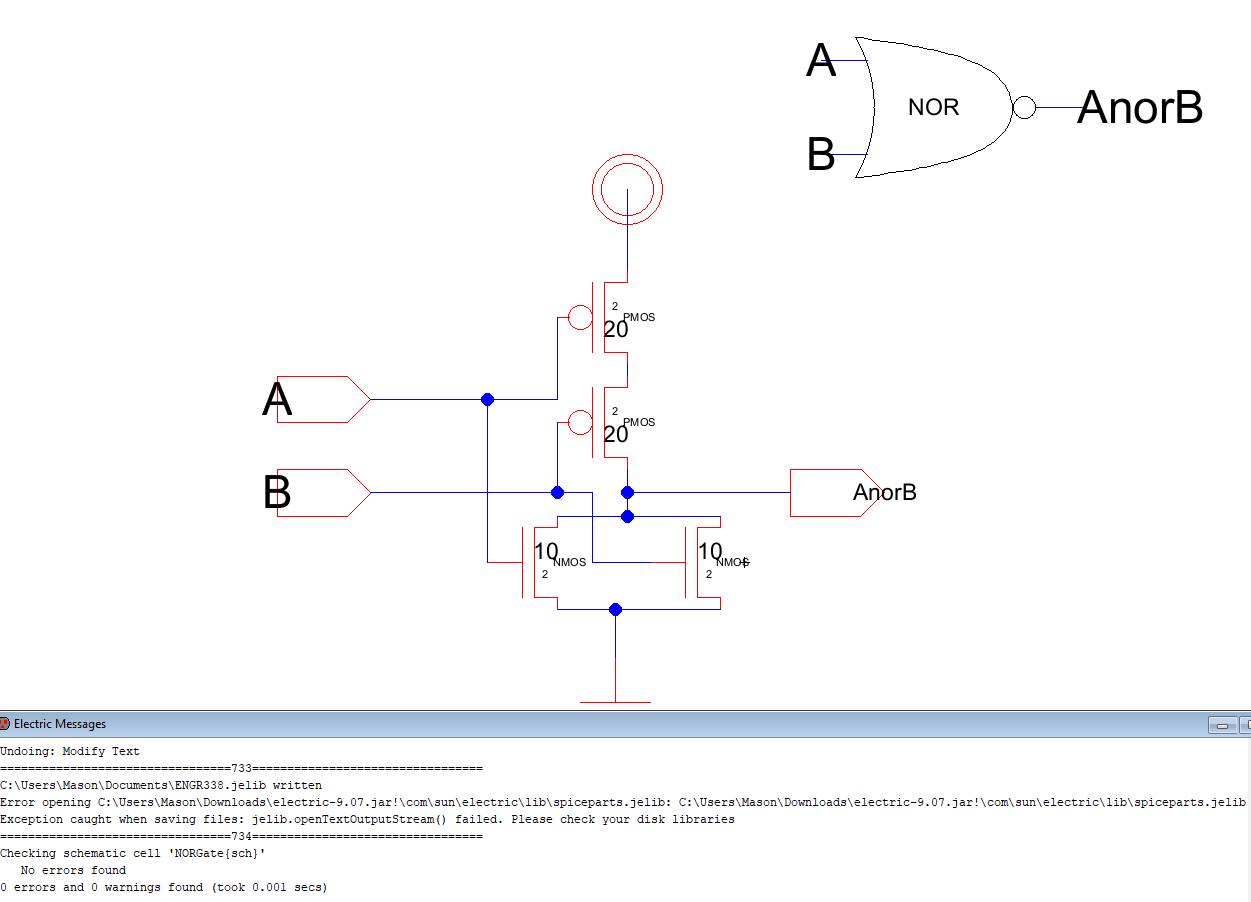
Figure 4. NOR Gate
schematic and icon.
This process went fairly smoothly with no issues.
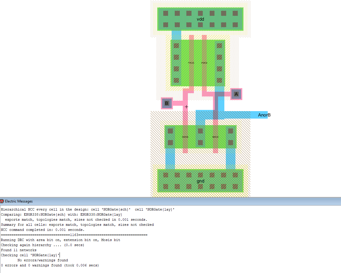
Figure 5. NOR Gate
Layout.
The final gate needed for the Full Adder was an Xor gate. This gate was
layed out using NMOS and PMOS gates. Two inverters were created since
both A and Anot as well as B and Bnot are needed for the Xor gate. The
schematic for the Xor gate can be seen below in Figure 6.
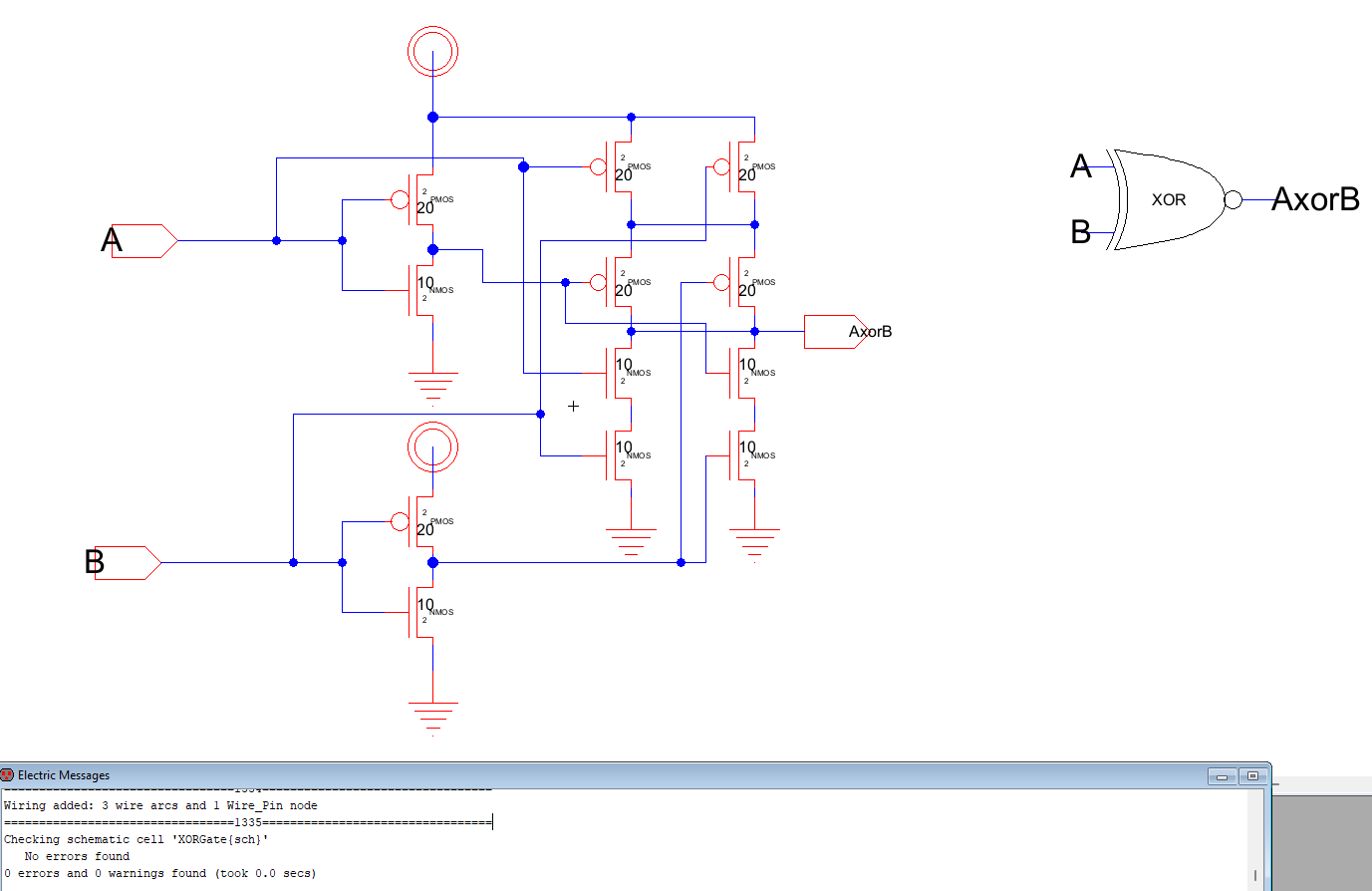
Figure 6. Xor
gate layout with clean DRC check.
A stick diagram was used to layout the Xor gate layout before going
into electric. I tried to use different colors but it ended up
confusing me more.
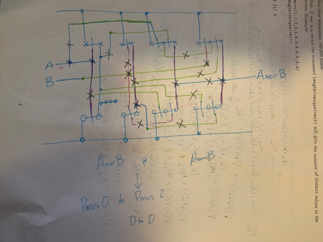
Figure 7.
Stick diagram for Xor Gate(on a stats exam, I ran out of paper).
The schematic was then layed out... several times... way too many times
to be proud of it but I finally finished the layout and it can be seen
below in Figure 8.
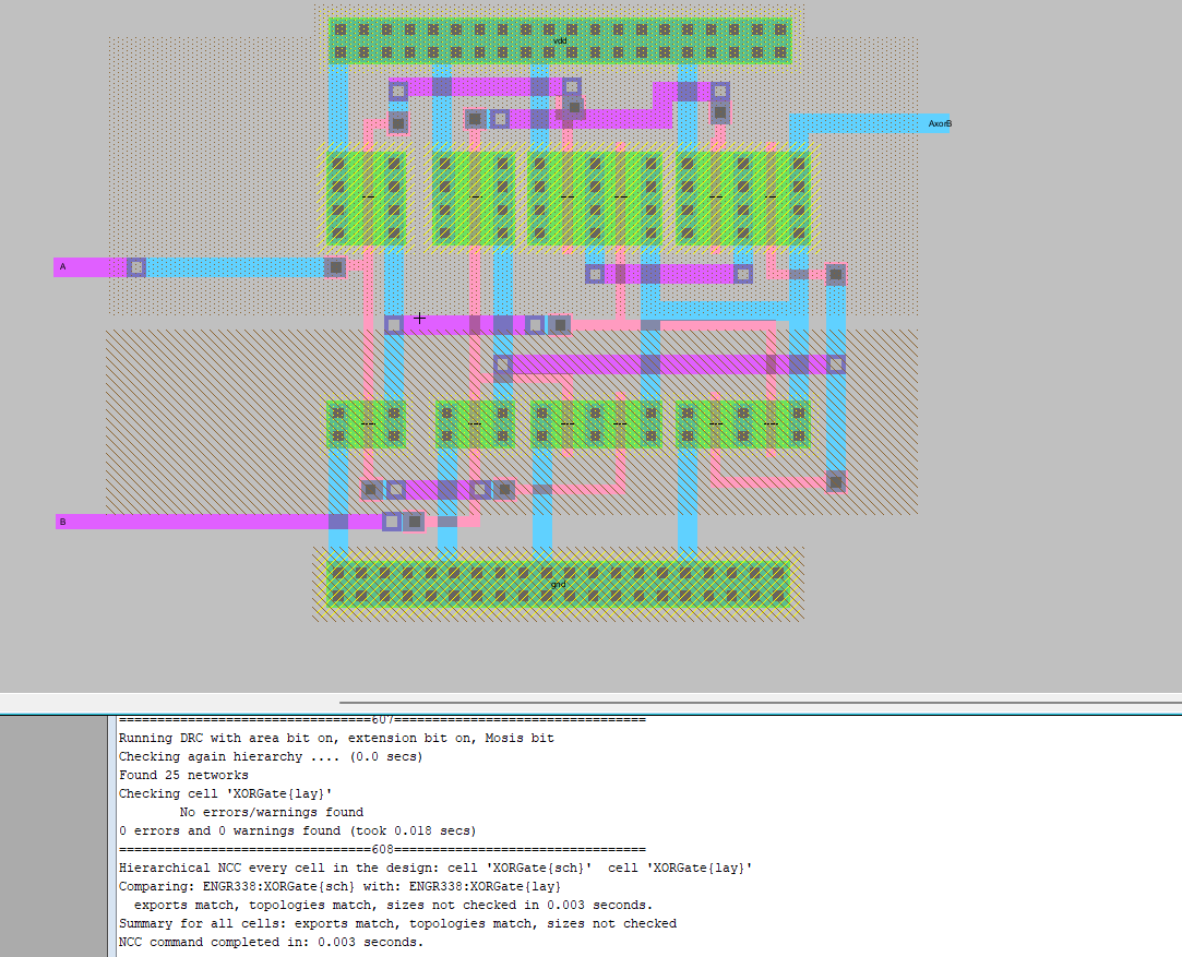
Figure 8. XOR
Gate Layout with Clean NCC and DRC!
The final step of this lab was to make the full adder. This was a lot
easier than I thought it would be. The schematic was layed out as seen
below in Figure 9. The logic was found on a tutorial posted to
yilectronics.com.
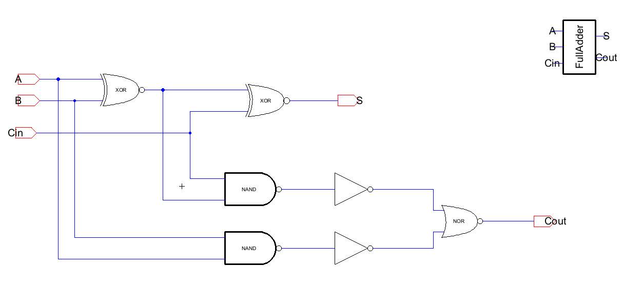
Figure 9. Full
adder schematic.
The final and most daunting task of the lab was the layout for the full
adder. This was also a lot easier than I expected since all of the
gates were known to work they just had to be wired together the final
layout can be seen in Figure 10.
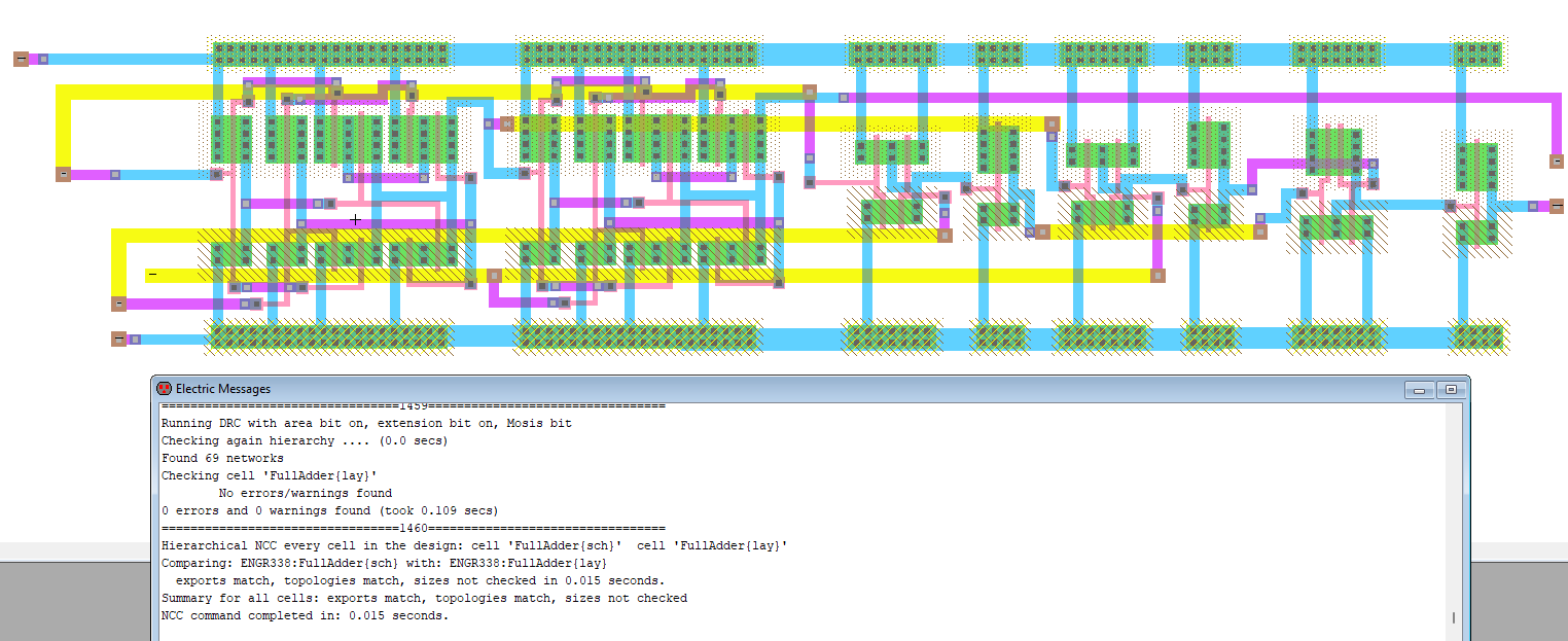
Figure 10. Full
adder layout.
All of the aformentioned circuits except the Full adder were simulated
driving a 100f capacitors to ensure the logic was correct and can be
seen in the results section. The full adder was also simulated below in
the results section.
Results:
As mentioned above the NAND, NOR, and XOR gates were simulated driving
a 100fF capacitor as seen below in Figures 11-13.
Figure 11. Simulation
results
for the NAND gate wired to a 100fF capacitor.
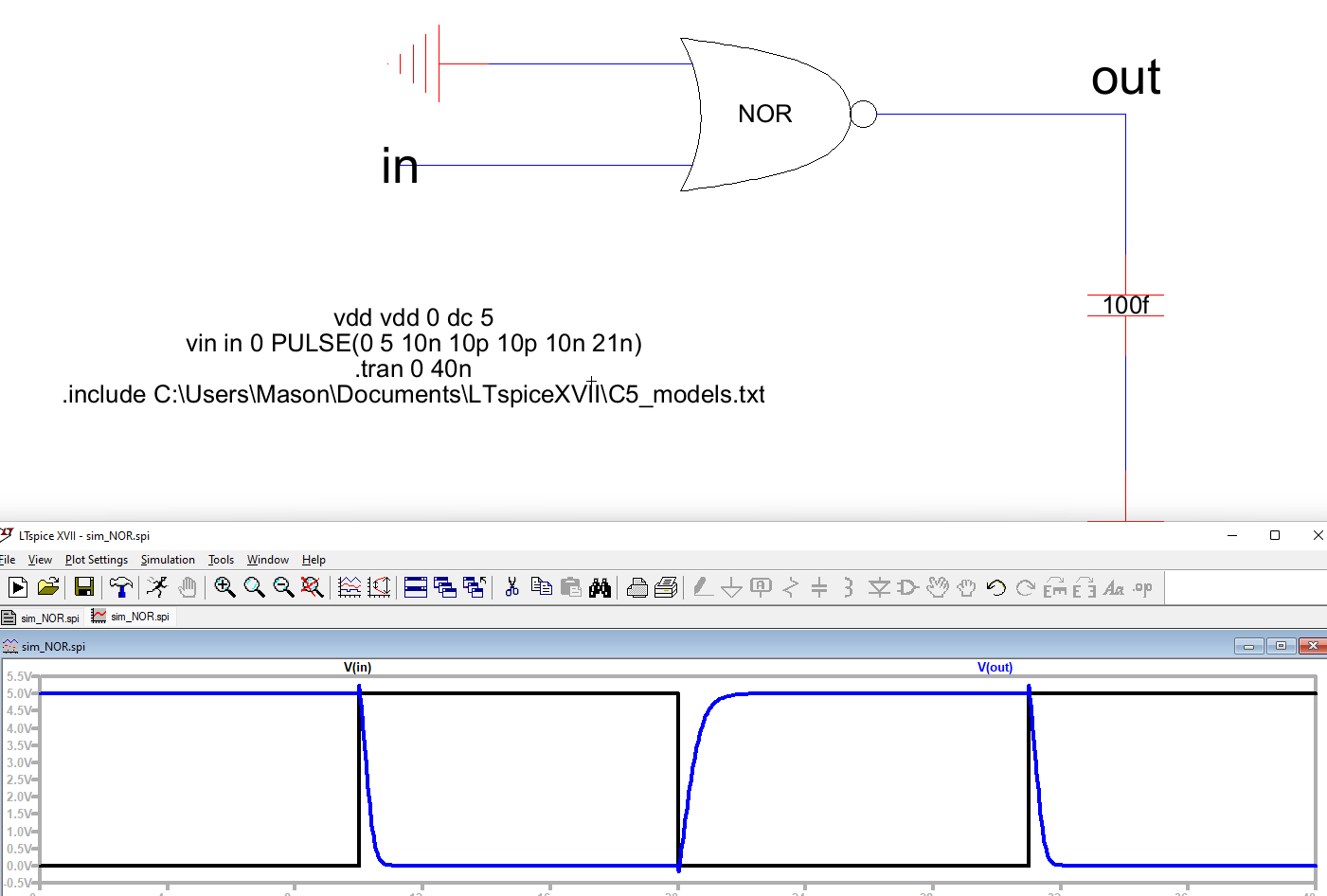
Figure 12. Simulation
results
for the NOR gate wired to a 100fF capacitor and ground.
And finally the XOR gate.
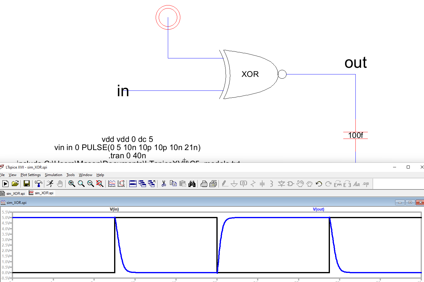
Figure 13. Simulation
results
for the XOR gate wired to a 100fF capacitor and VDD.
The
XOR gate was then wired to VDD to ensure the logic was working.
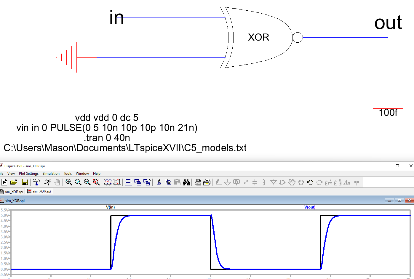
Figure 14. Simulation
results
for the XOR gate wired to a 100fF capacitor and GND.
Finally, the
full adders logic was simulated
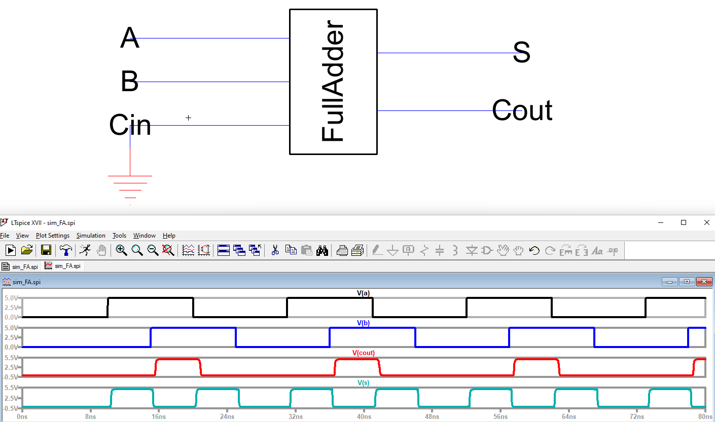
Figure 15. Simulation
results
for the Full adder with Cin shorted to ground.
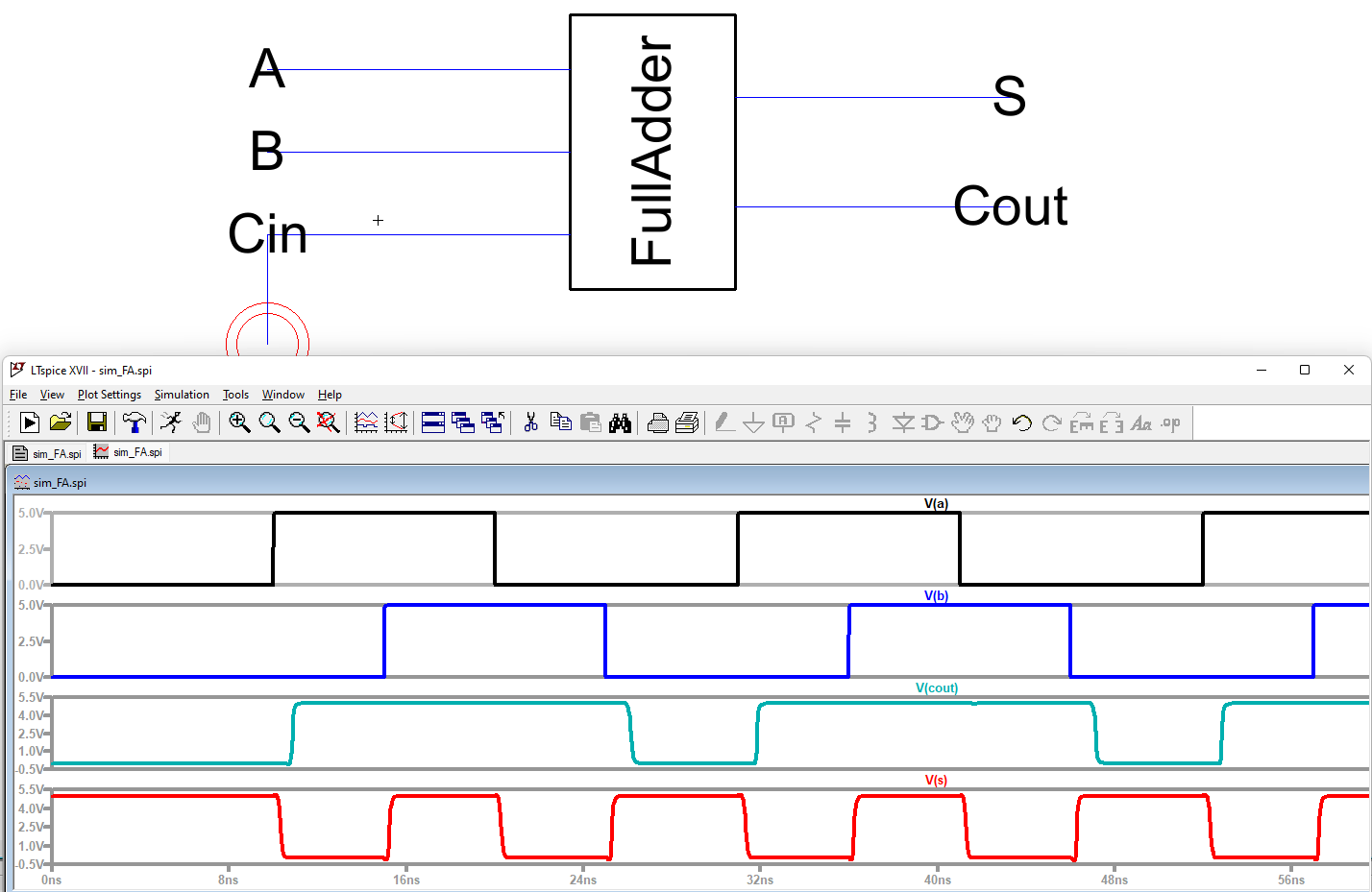
Figure 16. Simulation
results
for the Full adder with Cin shorted to VDD.
Discussion: Holy
cow did these layouts get complicated really fast. I had a lot of
errors with Electric not wanting to boot so I had to wipe my settings a
few times in the registry. I also had to do this in SEVERAL sittings as
to not get too frustrated. At the end of the day none of it was too
technically complex it was just very easy to miss things and the
debugger for NCC wasn't always the most useful.