ENGR338 Lab 2022
Fall
Lab 5 The
Inverter
Name: Mason
Brady
Email:
mrbrady1@fortlewis.edu
The
Inverter
Introduction:
This lab uses Electric VLSI and LTSpice to simulate pmos and nmos gates
in order to create an inverter.
Materials:
LTSpice, Electric VLSI
Methods:
First, an NMOS with size 10/2 and a PMOS with size 20/2 were placed in
series. A voltage source and ground were placed accordingly and
off-page connectors were placed between the transistors to complete the
circuit. An icon view was created and a DRC check was performed as seen
in Figure 1.
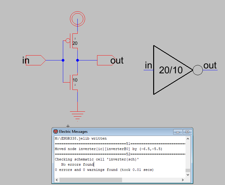
Figure 1.
Inverter Schematic and Icon with 0 DRC Errors.
The circuit was then simulated in LTSpice as seen in Figure 2.
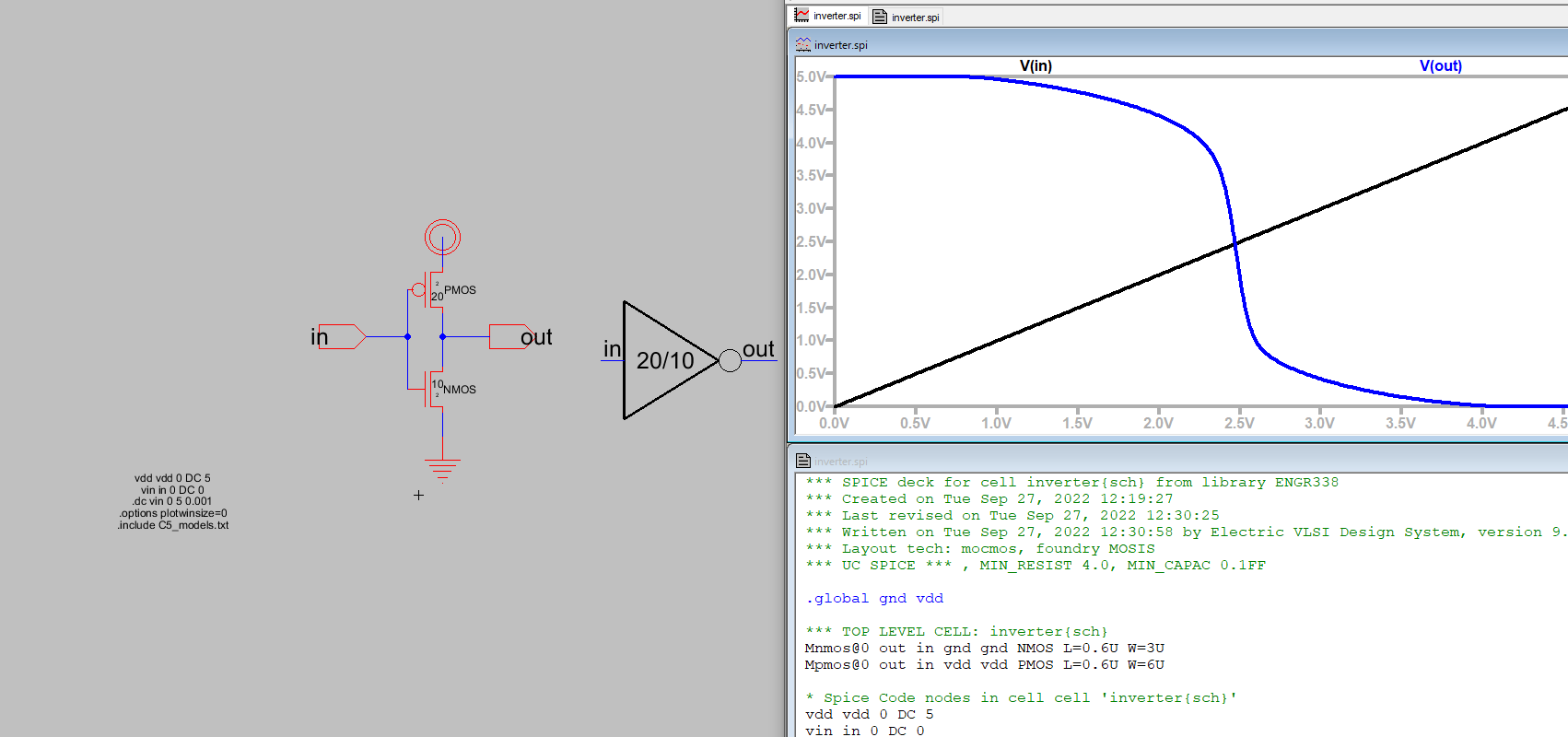
Figure 2. Inverter
Simulation.
A transient analysis using a pulse function was then run which can be
seen below in Figure 3.
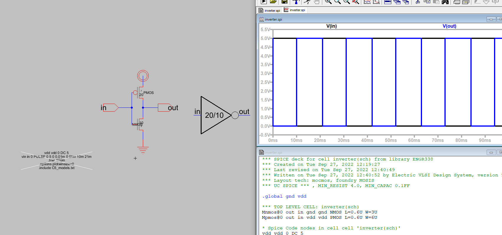
Figure 3. Inverter
Pulse Simulation.
The layout was created for the schematic which went fairly smoothly
with few issues and can be seen below in Figure 4.
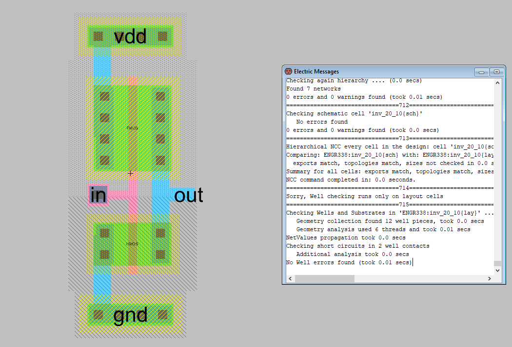
Figure 3. Inverter
Schematic with Well Check, DRC, and NCC complete.
The inverter was then multiplied by creating a duplicate schematic and
using the Spice multiplier function to create an inverter with M=5
forming a 100/2 and 50/2 inverter by putting 5 of our previous
inverters in parallel(I forgot to grab a screengrab of the schematic).
The layout was then completed by copying the previous schematic 4
times. The VDD and GND rails width was increased to encompas the
circuit and all of the transistors were wired as seen below in Figure 4.
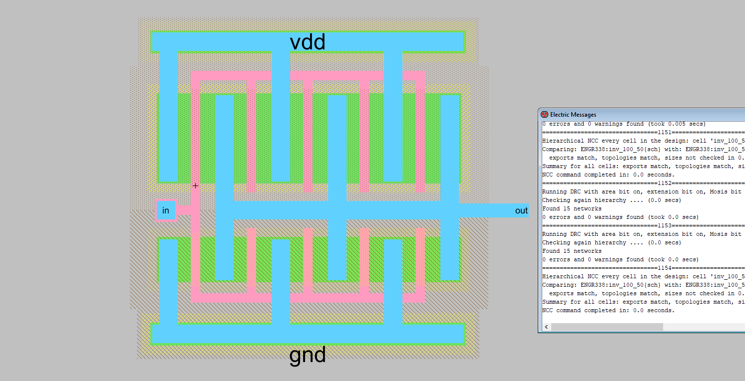
Figure 4. Inverter
Schematic with Well Check, DRC, and NCC complete.
The circuits were
then wired to drive various capacitors to compare the maximum current
through the two gates.
Results:
Both circuits were wired to drive a 100fF capacitor, the results can be
seen below in Figure 5 and 6.
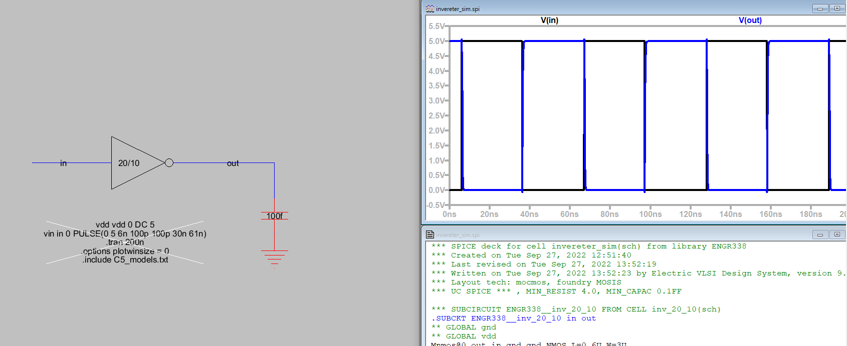
Figure 5. Simulation
results
for the 20/10 inverter gate wired to a 100fF capacitor.
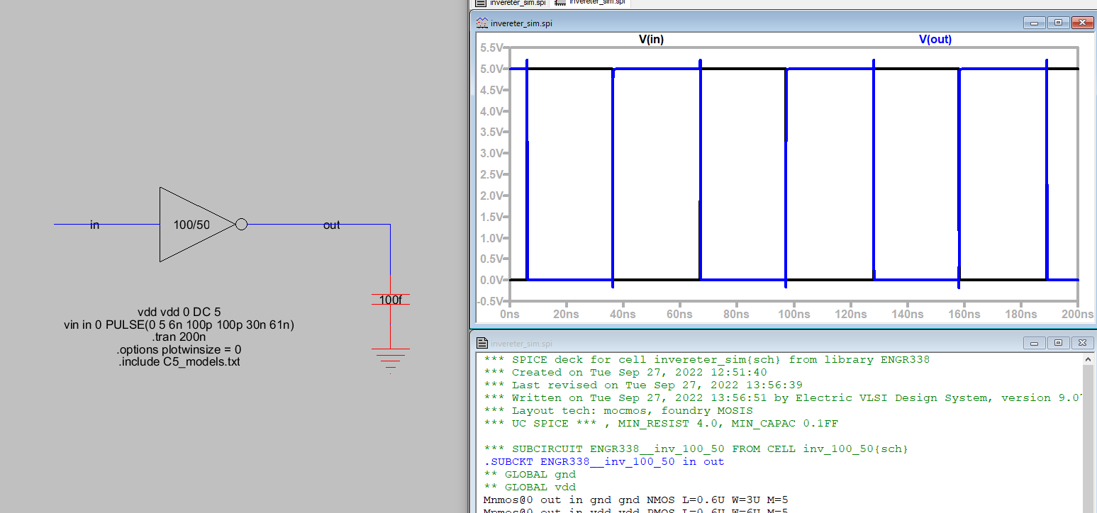
Figure 6. Simulation
results for the 100/50 inverter gate wired to a
100fF capacitor.
Both circuits were then wired to drive a 1pF capacitor, the results can
be seen below in Figure 5 and 6.
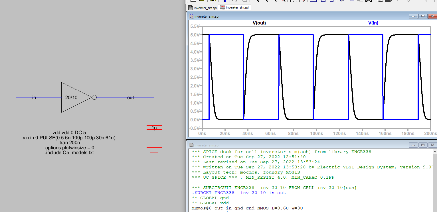
Figure 7. Simulation
results
for the 20/10 inverter gate wired to a 1pF capacitor.
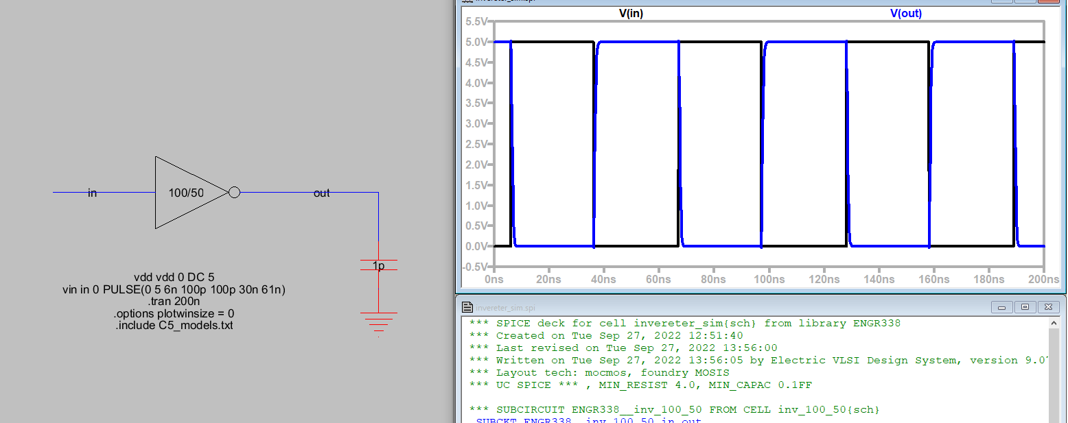
Figure 8. Simulation
results for the 100/50 inverter gate wired to a
1pF capacitor.
Finally, both
circuits were wired to drive a 10pF capacitor, the results can be seen
below in Figure 9 and 10.
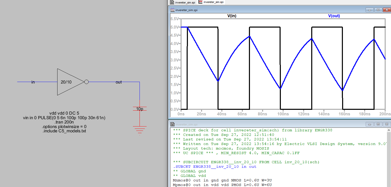
Figure 9. Simulation
results
for the 20/10 inverter gate wired to a 100fF capacitor.
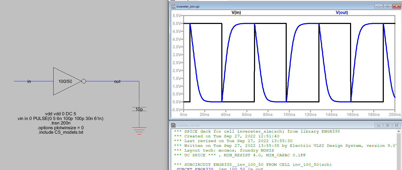
Figure 10. Simulation
results for the 100/50 inverter gate wired to a
10pF capacitor.
Discussion: This lab was fairly
straightforward once the correct spacing was achieved for the 100/20
inverter. I found the easiest approach to getting the spacing right was
to use the info panel and adjust the x position through that.
Otherwise, this lab was fairly straight forward and the results self
explanatory.