Embedded Systems
Spring 2024
HW 4 Data Storage
Name: Mason
Brady
Email:
mrbrady1@fortlewis.edu
HW 4
Introduction:
This homework is an introduction to Combinational Logic Blocks
Materials:
gvim, vivado, basys 3
1) SR Latch
The SR Latch uses S to set and R to reset. The
module and test bench are quite simple just detecting a change in
either pin and setting the appropriate q and q_not. The details of the
sub module, test bench, and simulation outputs can be seen in Figure 1
below.
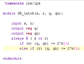
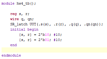
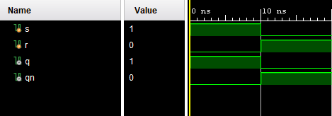
Figure 1. SR_Latch sub module, testbench, and simulation showing correct outputs for the two primary input cases.
2)SR Flip Flop
The
SR Flip Flop was a slight modification to the SR Latch so I coppied the
logic of the SR Latch into a new sub module and rewrote the test bench
to account for more cases. So far I prefer using for loops to generate
test cases because I find I tend to miss key edge cases when I hard
code them in so using the for loop lets me test every possible case
(most of the time) with very little code. The sub module, test bench,
and simulation can be seen below in Figure 2. If this was a rising edge
trigger, the clk needs to be the first bit otherwise it will ignore
most of the cases.
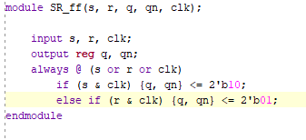
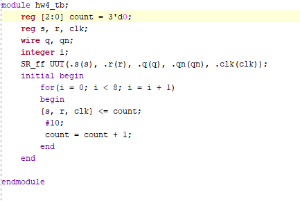

Figure 2. SR Flip Flop sub module, test bench, and simulation.
3)Edge Triggered D Flip Flop
The
edge triggered D flip flop was also pretty similar to the previous case
but instead of s, r we only have d and clr. Clr is the exact same as
the reset pin on the last case and could use the same logic (minus the
clk since we are already taking that into account). Otherwise, q is
just set to d and qn is set to dn. The sub module, test bench, and
simulation can be seen below in Figure 3.
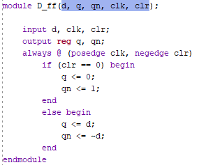
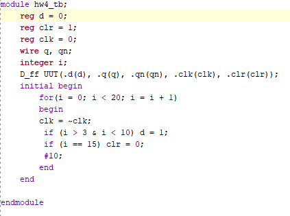
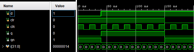
Figure 3. D flip flop sub module, test bench, and simulation.
4)Edge Triggered JK Flip Flop
The
JK flip flop is like a hybrid between the D and SR flip flops. It has
three inputs allowing for basically a D flip flop with an inversing
function (11). The testbench was setup nearly identically to the last
one just had to put clr as the first bit of the count converter. This
way the gate doesn't get reset on every other bit change, just after we
have looped through everything else.
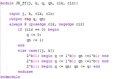
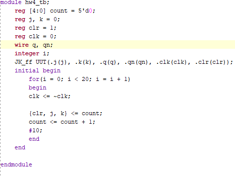
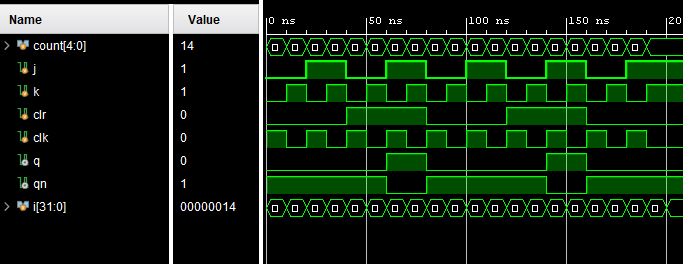
Figure 4. JK Flip Flop Sub module, test bench, and simulation.
5)T Flip Flop
The
T flip flop was slightly more interesting using an xor gate for the
logic. Other than that everything else is nearly identical. I had to
use a placeholder bit in the test bench so that clr and t would stay
the same for a full clock cycle. Another way to do this would be to add
clk <= ~clk; #10; after the #10 in the tb.
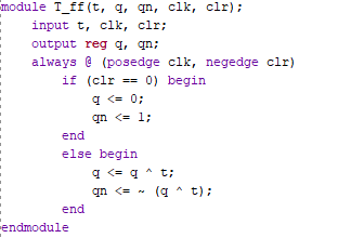
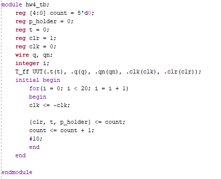
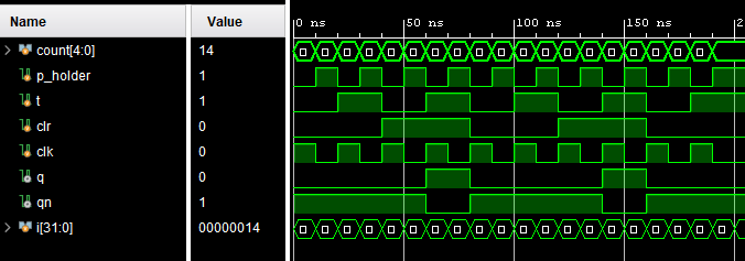
Figure 5. T Flip Flop sub module, test bench, and simulation.
6)ROM
The
Read Only Memory section of the homework was pretty cool. I started by
just writing the submodule and test bench given to us. The readmemb
operator and the definition of the memory register was new but the rest
of this was pretty routine. The memory is defined as 256 8-bit
registers which stores the memory from the storage file read in by
$readmemb (read memory binary). The test bench was also pretty standard
to how I have been setting up my test benches except for the $monitor
which I still don't really understand. The % is clearly a variable
string fill (the syntax and usage is very similar to what I have been
doing with HTML strings for senior sem which was neat).
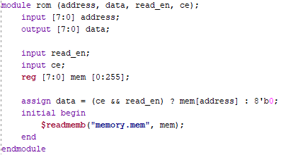
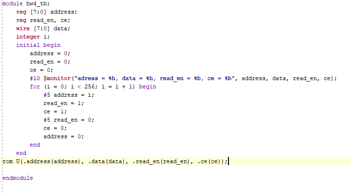
Figure 6. ROM submodule and test bench.
I generated a memory file by copying a bunch of 8 bit binary
strings and then randomly changing bits. This creates a semiperiodic
list fairly quickly. For room and my own sanity I'm only displaying the
first 33 numbers in the memory and the first 120ns of the simulation.
As you can see they line up with every other clock cycle being a 0
since it takes 2 cycles to read the memory.
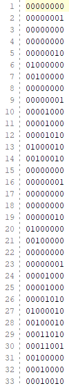
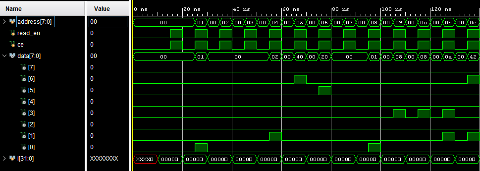
Figure 7. ROM file and simulated read showing matching output to input.
I
then did the same thing with 4 hex numbers or 16 bits. All that I had
to change is the number of bits read in, the adress length, and the
length of read in. For the next few demonstrations these are the only
things to change between the files which made it quick to write. I am
not going to talk about the rest of these too much because they are all
almost identical except for changing the length of memory and the
length of the stored info.
The readmem function also needs to be
changed to read in hex or it will be confused. For this first example
in Figure 8, I used the same memory file in the demonstration but I
forogt to screen grab it before oberwriting it with the next example.
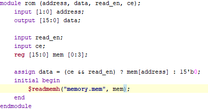
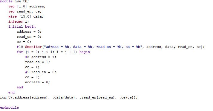
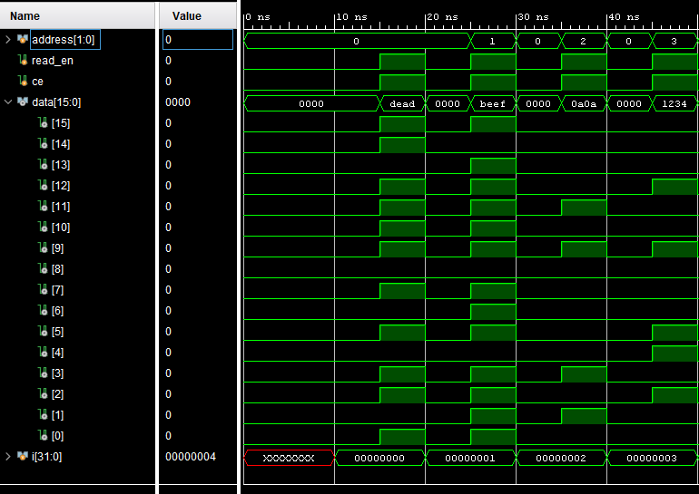
Figure 8. ROM Hexidecimal read in sub module, test bench, and simulation.
Then I set it up to read in more 2 digit hex numbers, as seen in Figure 9.
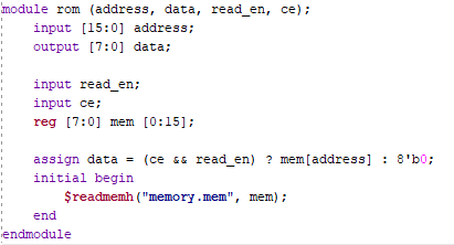
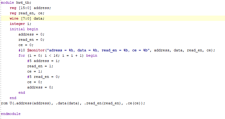
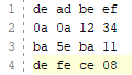
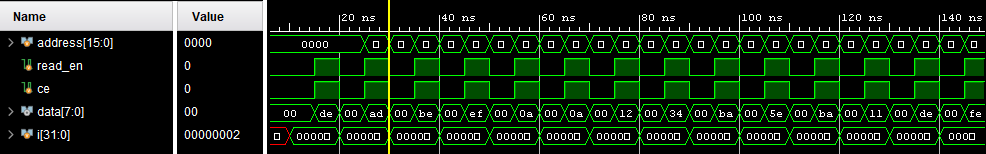
Figure 9. ROM
submodule, test bench, memory file, and simulation output. The output
clearly shows the same values as the input sepearated by the 00 bit of
the first clock cycle.
And I modified the code one more time to do 3bit binary numbers.
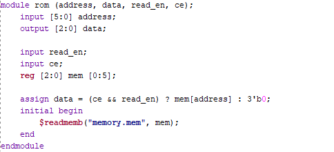
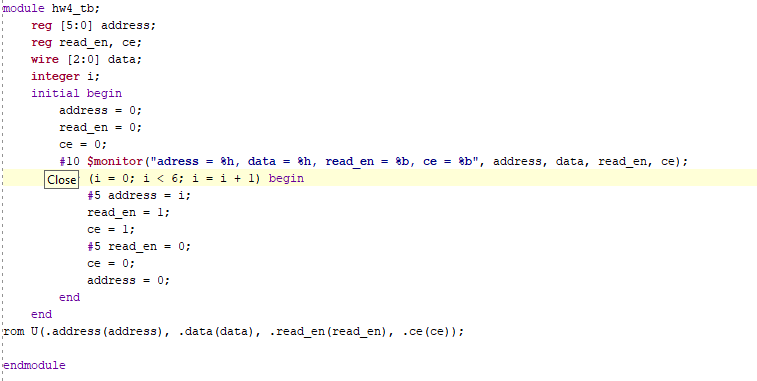

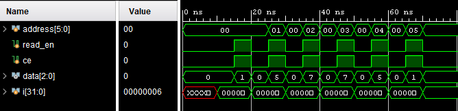
Figure 10. ROM 3-bit binary sub module, test bench, memory file, and simulation.
Finally
I had to use the IP ROM, I first set up my for loop to only increment
by one but because of how the memory file is setup this resulted in
pretty poor results as seen in Figure 11.
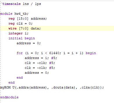
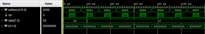
Figure 11. IP ROM test bench and simulation.
Because
of this I changed the iteration step size to 50 and this gave results
that showed it was actually reading the memory file provided.

Figure 12. IP ROM simulation with corrected step size.
Breadboard Debounce
I
wired the breadboard debounce and the circuit was pretty simple, I just
had an issue of not grounding my oscilliscope (Thanks Dr. J)
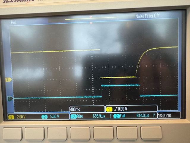
Figure 13.
Breadboard debounce circuit output. The blue line is the debounce
output and the yellow line is at points 1/2(identical output).
Discussion:
This
weeks work felt very long and some of the tasks felt repetitive and
redundant (Doing MUX several times and the large version of simple
gates). Other than that the code was striaght forward, just seemed like
it didn't stop. I also got very lazy with the writeups towards the end.