Lab3: More FPGA
Name: Lucien Verrone Email:
ljverrone@fortlewis.edu
Introduction:
This assignment was a deeper
dive into FPGA programming. This lab required the programming of an
inverter, a 2-bit full adder, an 8-input AND gate, and a 4-1 MUX along
with physical simulations for each Along with this, the lab experements
with timing using the onboard clock and with using the onboard
seven-segement display as an output.
Task 1:
Task one was to create an
inverter, a 2-bit full adder, an 8-input AND gate, and a 4-1 MUX. Along
with this, I was also required to simulate each gate.
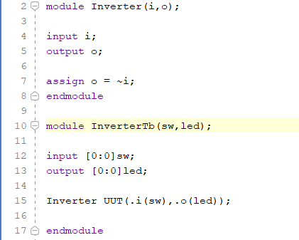
This inverter simply assigns the output to ~input.
Figure 1: inverter code.
Figure 2: inverter demonstration.
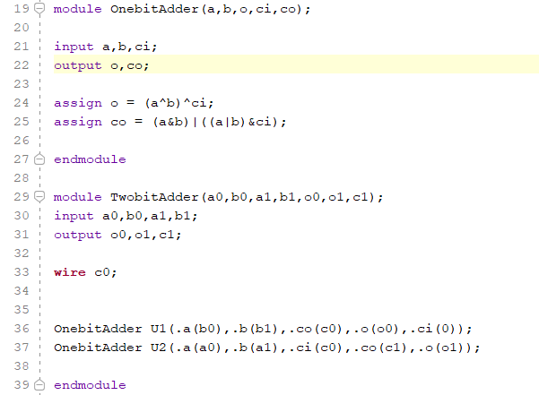
This 2-bit full adder uses two one bit adders to accomplish two bit
binary addition. The least significant bits are added first, and the
carry out from that one bit adder is connected to the carry in for the
second one bit adder which adds the most significant bits. In my
physical representation, switches one and zero make up two bit number
one while switches three and two make up two bit number two (ie. 1010 =
10 + 10). The output is made up of three LEDs. LEDs one and zero make
up the two bit output, while LED 2 is the carry out for the two bit
adder.
Figure 3: 2-bit full adder code.
Figure 4: 2-bit full adder demonstration.
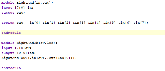
This 8-input AND gate simply takes an array of eight inputs and uses 2-input AND gates on each to achieve an 8-input AND gate.
Figure 5: 8-input AND gate code.
Figure 6: 8-input AND gate demonstration.
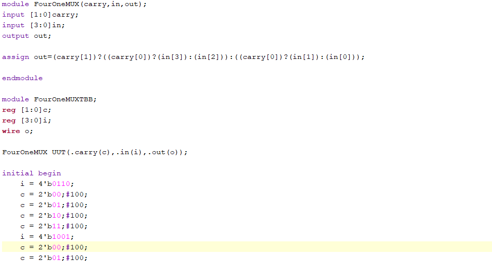
This 4-1 MUX uses embedded
conditions to achieve a 4-1 MUX gate. This is done by first looking at
the value of the second carry, then loooking at the value of the first
carry and finally assigning the relevent input to the output. Figure 7: 4-1 MUX code.
Figure 8: 4-1 MUX gate demonstration.
Task 2:
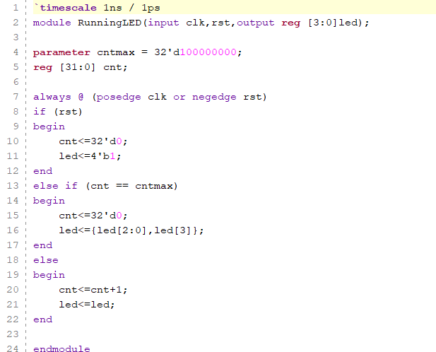
Task two was to create a program that demonstrates the onboard clock by toggling LEDs at a variable of one second.
To do this, the 100MHz
onboard clock was counted 100 MEG (100*10^6) times per toggle to
achieve one second per event. The program also included a reset switch
to reset the counter. At each positive edge of the clock or negative
edge of the reset switch, the program will either reset if the reset
switch is toggled, add one to the count, or toggle the next LED if the
count equals the 100 MEG max set. Figure 9: Running LED code.
Figure 10: Running LED demonstration.
Task 3:
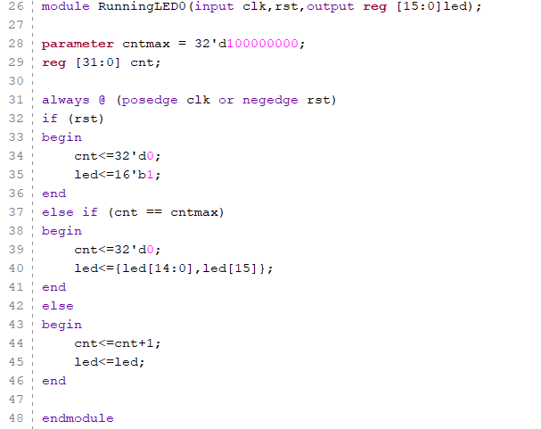
Task three was to modify the Running LED program from task two to use all 16 LEDs rather than just four.
This was done simply by increading the size of the LED register to sixteen from four. Figure 9: Running 16-LED code.
Figure 10: Running 16-LED demonstration.
Task 4:
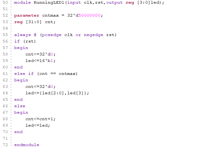
Task four was to modify the Running LED program from task two to toggle at a frequency of half a second rather than one second.
To do this, I simply halved the maximum count varaible. Figure 9: Running LED code at one half second.
Figure 10: Running LED demonstration at one half second.
Task 5:
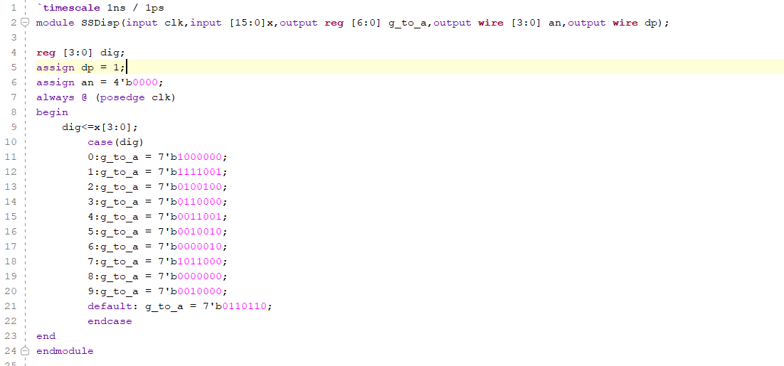
Task five was to use four switches as binary inputs to display a one digit decimal number on all of the seven segment displays. Figure 9: Seven-segment diplay code.
Figure 10: Seven-segment diplay demonstration.
Task 6:
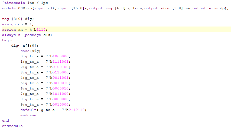
Task six was to recreate the
program in task four, but insead of using all four of the seven segment
displays only one is needed. This was done simply by changing the an value from 4'b0000 to 4'b1110. Figure 11: Seven-segment single display code.
Figure 12: Seven segment single display code demonstration.
Task 7:
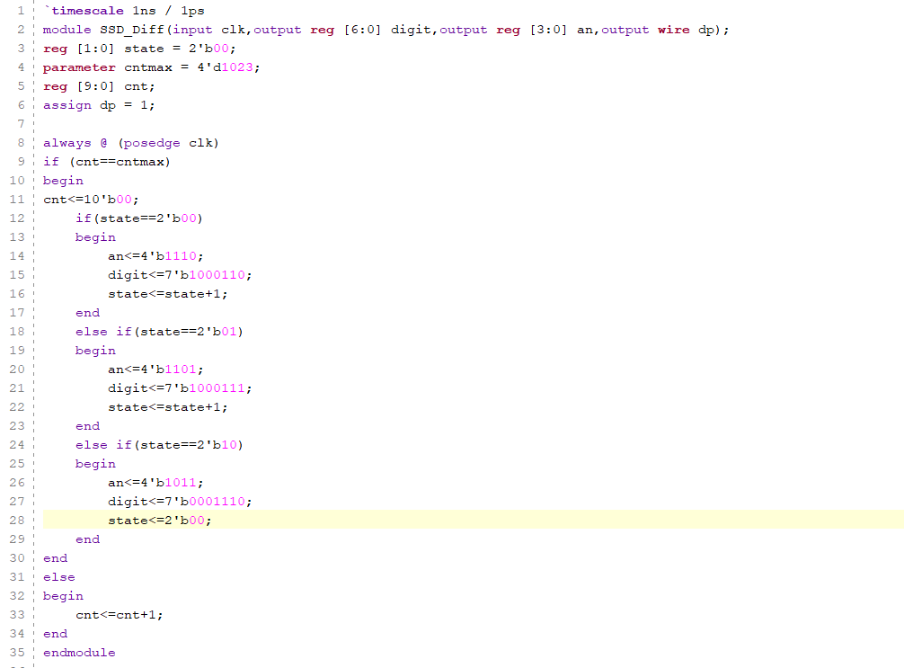
Task seven was to display
"FLC" on three of the seven segment displays. To do this, because each
display is connected, changing the value of an between each letter
based on the embedded clock was required. This was done using a
sensitivity list and if-else statements. Figure 13: Seven-segment "FLC" code.
Figure 14: Seven-segment "FLC" demonstration.
Task 8:
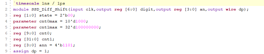
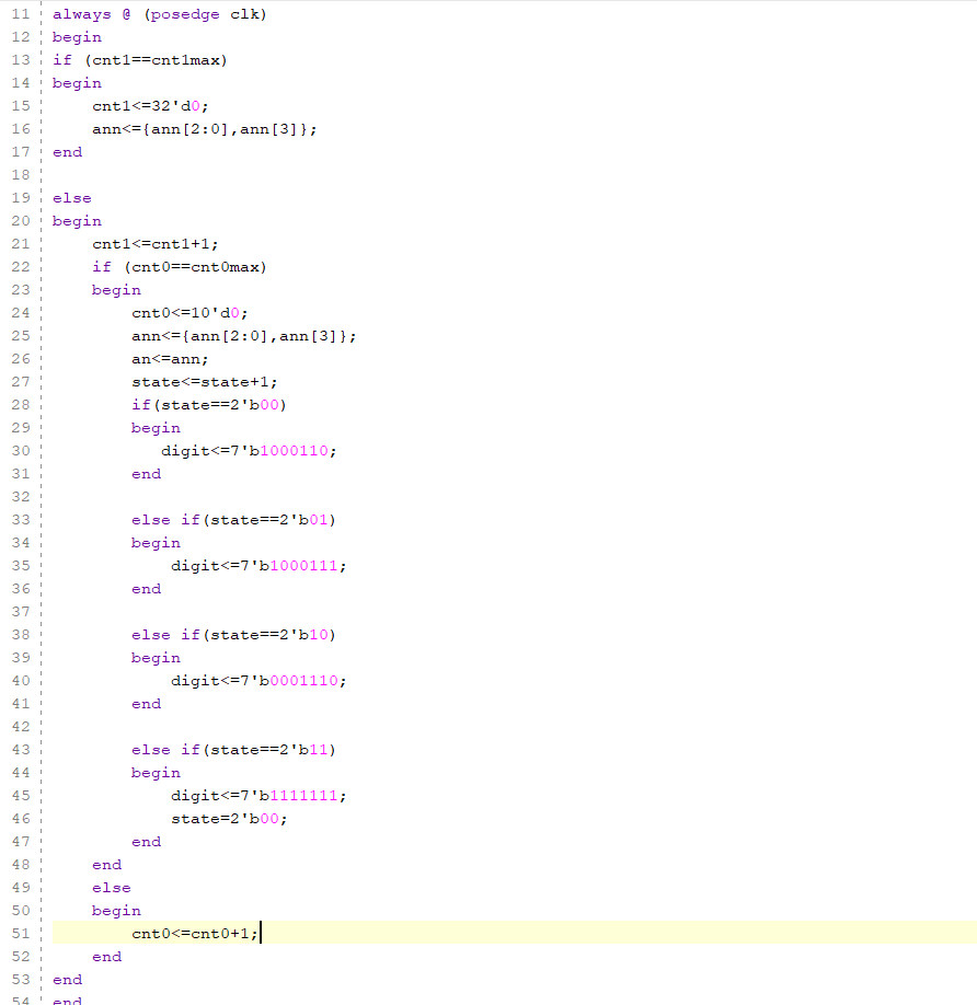
Task eight was to modify the program from task seven to have "FLC" shift from right to left.
This was much more complicated due to needing not only a shift of the
three active seven-segment displays but also a shift for each letter
within these three active displays. This was done by having two
counters, one with a larger max value that triggers a shift of bits in
an along with a counter with a smaller max value that shifts the bits
and updates the state for each letter. Rather than having a state for
each letter like the program in task seven, an extra blank state was
also required to ensure the smaller counter shifts of an don't interfere with the the larger counter shifting the whole word. Figure 15: Shifting seven-segment "FLC" code.
This assignment challenged my
understanding of FPGA programming and Verilog. While the first few
tasks were generally straight forward, the seven segment display
challenged me. The combination of a new component I was unfamiar with
and a programming environment I am unfamiliar with threw me for a loop,
and I spent a while flipping bits and trying to troubleshoot my logic.
In the end, my anode bits were assigned to one rather than zero. While
troubleshooting this, however, I learned a lot about using seven
segment displays. Task one was straightforward and took a little bit of
time to think through logic tables and embedded modules, while tasks
two and five was easy as a fill in the blank scaffold was provided.
Tasks seven and eight required some deep thought about the order of
operations within functions along with detailed timing work.