This assignment was an
intro into FPGA programming and more experience simulating in Vivado.
Tasks included writing code in Vivado modeled off of the code shown
in class, creating test benches to simulate in Vivado, and pushing .bit
and .bin files for volatile and non-volatile storage.
Task 1:
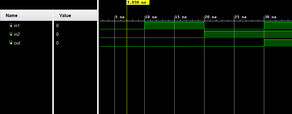
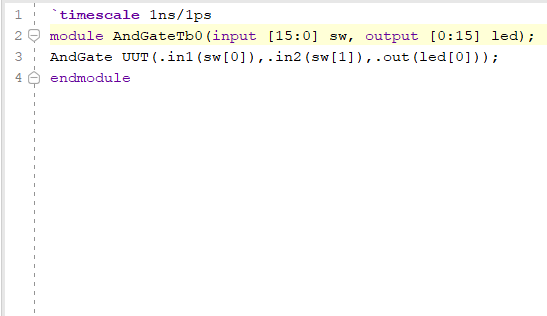
Task one was to code an AND
gate in Vivado along with a test bench. The test bench was then
simulated to ensure finctionality before being edited to function on
the FPGA board by changing the input ports to writeches and the output
port to an onboard LED. The edited code is sythesised into .bit and
.bin files before being uploaded to the FPGA board in bitstream format
and binary format.
Figure 1: (Left to right) AND gate simulation code, simulation results, FPGA code.
Figure 2: FPGA AND gate demonstration.
Task 2:
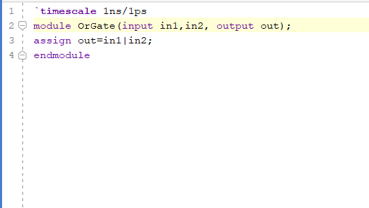
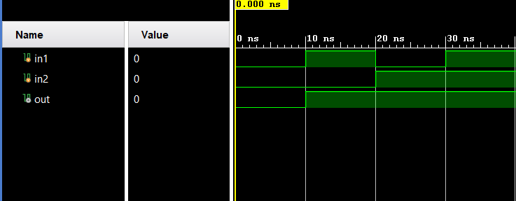
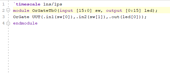
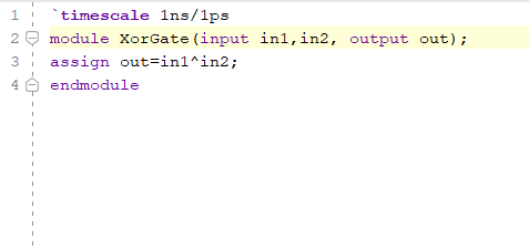
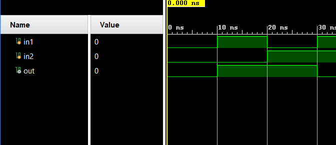
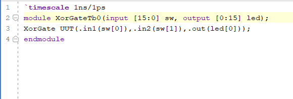
Task two was to implement an
OR and XOR gate along with test benches and FPGA compatible code,
replicating the process in task one.
Figure 3: (Left to right) OR gate simulation code, simulation results, FPGA code.
Task three was to demonstrate
the difference between volatile and non-volatile storage on the FPGA
board. This was done by loading the AND gate to the non-volatile
storage and loading the OR gate to the volatile storage, then switching
between the two.
Figure 7: Volatile/non-volatile demonstration.
Discussion:
This assignment was a good introduction to inplementing Vivado code on a FPGA
board. This process included augmenting code to be compatable with the
FPGA pins and ports. It also included trouble shooting some connection
issues I had with the FPGA board. Overall, I feel very prepared to take
on coming labs involving the FPGA board and I am excited to see the
more complex things the board can do.