This assignment required working with the VGA port output on the FPGA board in various ways, along with clock modules.
Task 1:
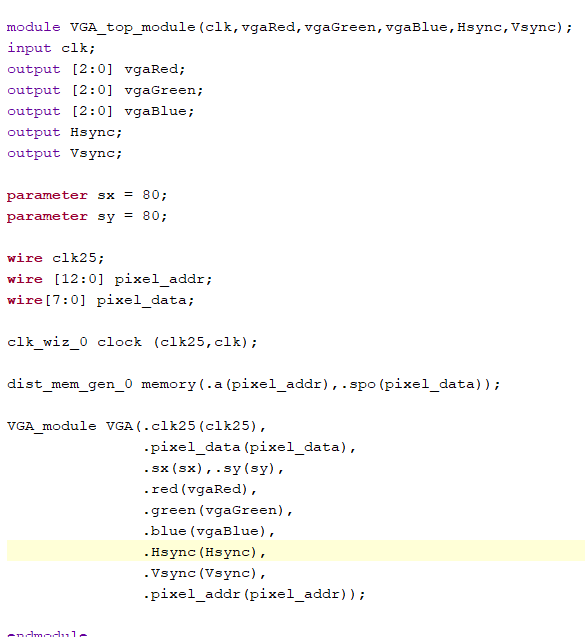
Task one was to recreate a
VGA program from the textbook. This program uses a clock generator IP
at 25MHz and a distributed ROM loaded with a test image COE file.
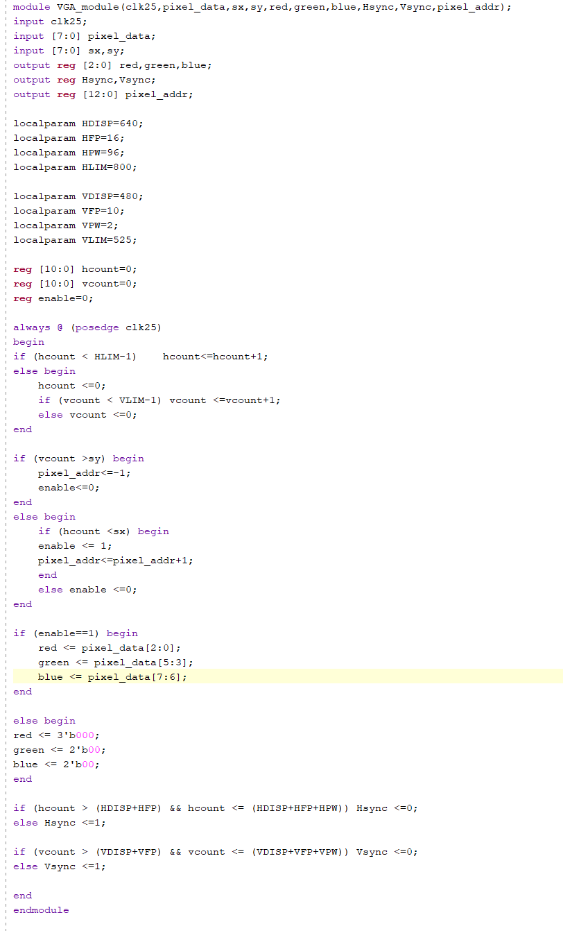
Figure 1: VGA program code
Figure2: VGA program demonstration
Task 2:
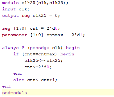
Task two was to replace the clock generator IP with a clock driver module with the same frequency Figure 3: 25ms clock module.
Figure 4: Demonstration with 25ms clock module.
Task 3:
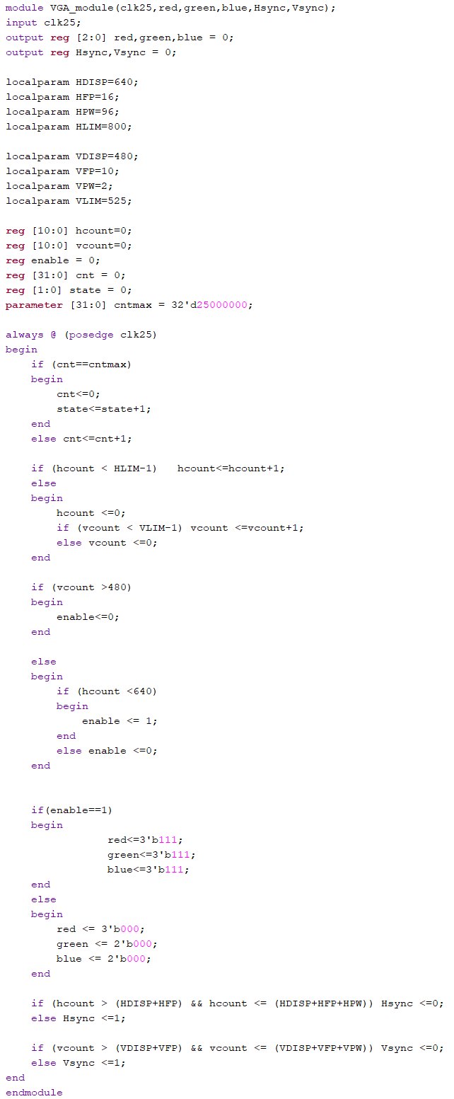
Task three was to modify
the module from task two to display an entirely white screen, and then to create a module that cycles RGB on the whole screen.
Figure 5: White VGA code, the same VGA_top_module was used as above.
Figure 6: White VGA demonstration.
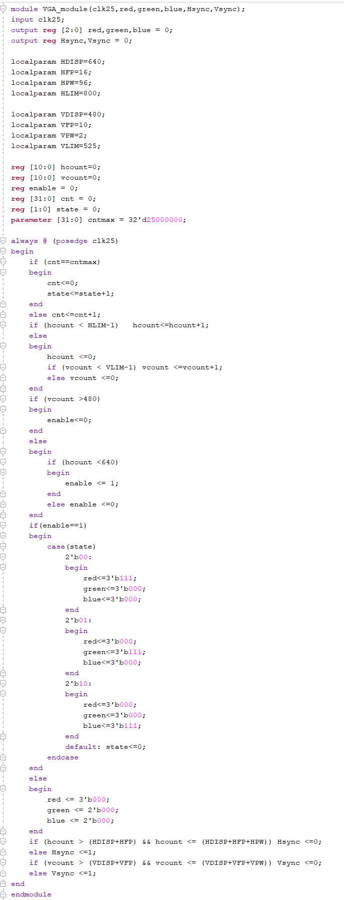
Figure 7: RGB cycle code.
Figure 8: RGB cycle demonstration, the same VGA_top_module was used as above.
Discussion:
This assignment gave me an
introduction to coding for VGA output in Verilog. The assignment was
straightforward, but nuances in the coding had me hung up for a while.
For example, when creating the white and RGB cycle code I attempted to
input sx and sy as the maximum screen size values but ran into constant
errors. The fix was to implement the constants directly in the VGA
module rather than having them as inputs. I still do not know why this
matters.