CE 433 Embedded Devices
HW4: Data Storage
Name: Lucien Verrone
Email:
ljverrone@fortlewis.edu
Introduction:
This assignment was an in
depth look at more advanced gates in Vivado, along with an introduction
to data storage. This assignment started with latches and flipflops,
before moving on to a button debounce circuit. After this, the
assignment continues with more flipflops and finally wraps up with an
introduction into memory and ROMs, including an introduction to IP
blocks.
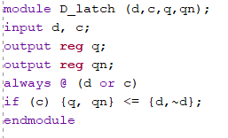
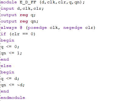
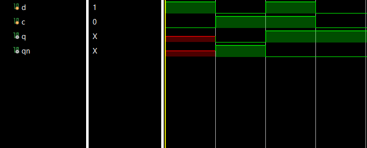
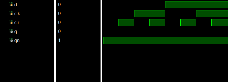
Task 1:
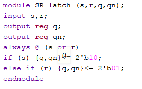
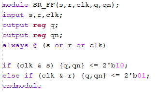
Task one was to recreate an
SR latch, SR flip-flop, a D latch, and an edge triggered D flip-flop
along with simulating each module virtually.
Figure 1: SR latch and SR flip-flop code.
Figure 2: SR latch and SR flip-flop simulations.
Figure 3: D latch and edge triggered D flip-flop code.
Figure 4: D latch and edge triggered D flip-flop simulations
Task 2:
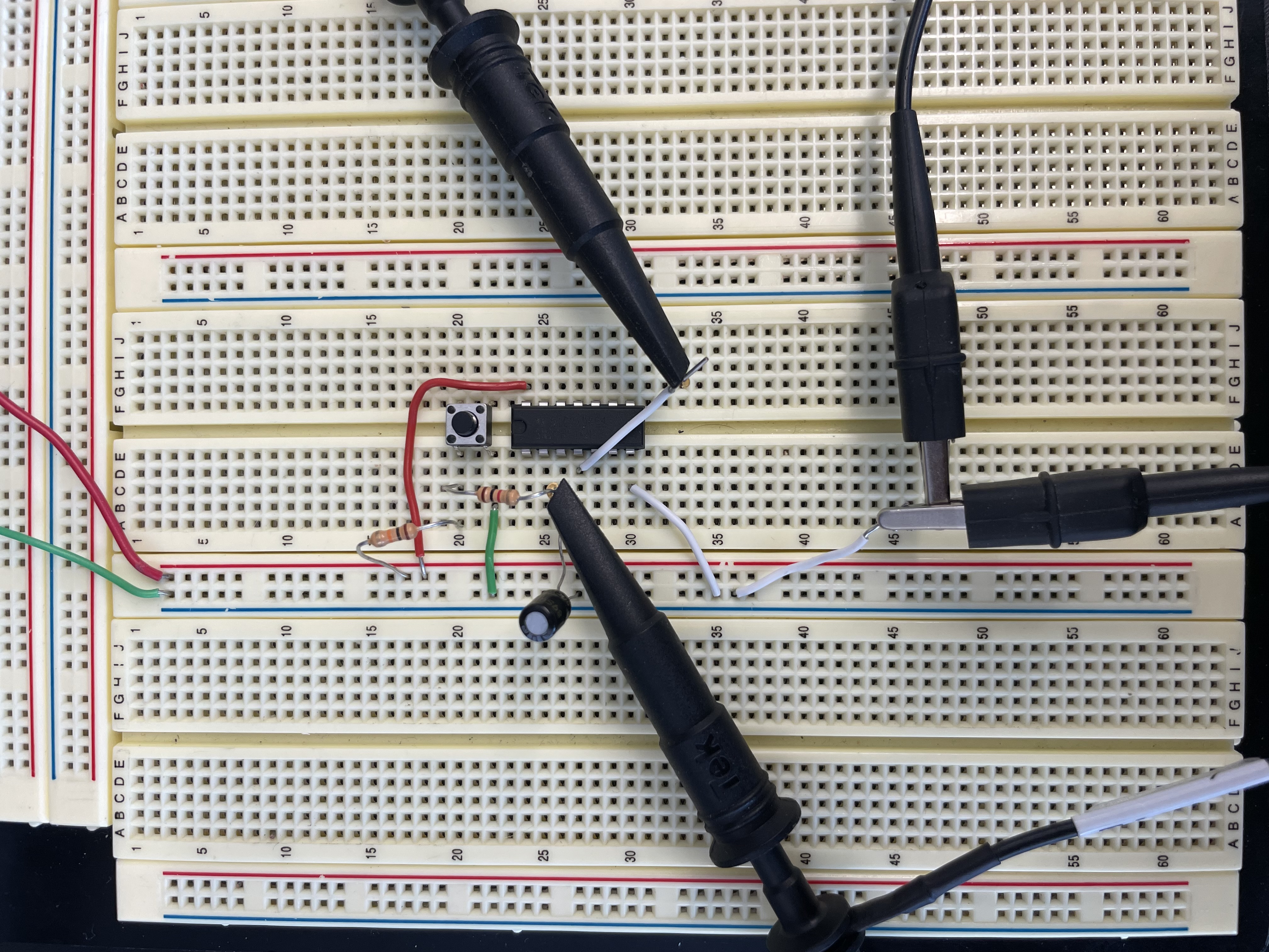
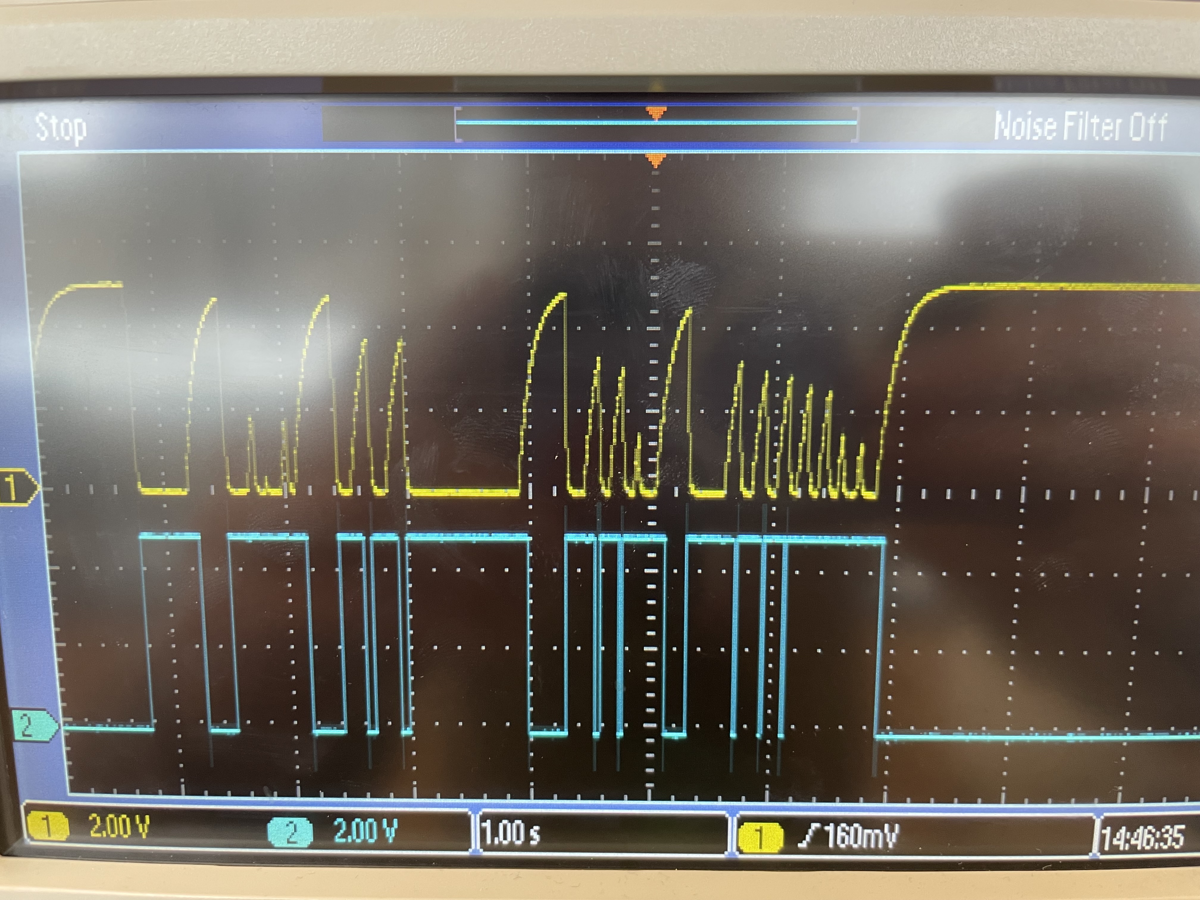
Task two was to implement a
button debounce circuite on a breadboard and test it using a DC source.
The circuit consisted of two resistors, a capacitor, and a Schmitt
trigger IC chip.
Figure 5: Button debounce circuit and oscilloscope reading (yellow is button input, blue is circuit output).
Task 3:
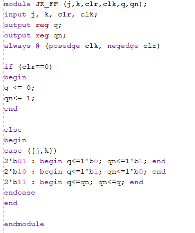
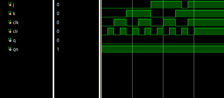
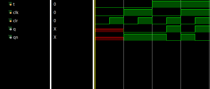
Task three was to implement a JK and T flipflop and simulate each.
Figure 6: JK and T flip-flop code.
Figure 7: JK and T flip-flop simulations
Task 4:
Task four was to experement
with reading different memory files, ending with building a ROM IP
block and designing and simulating a test bench for it.
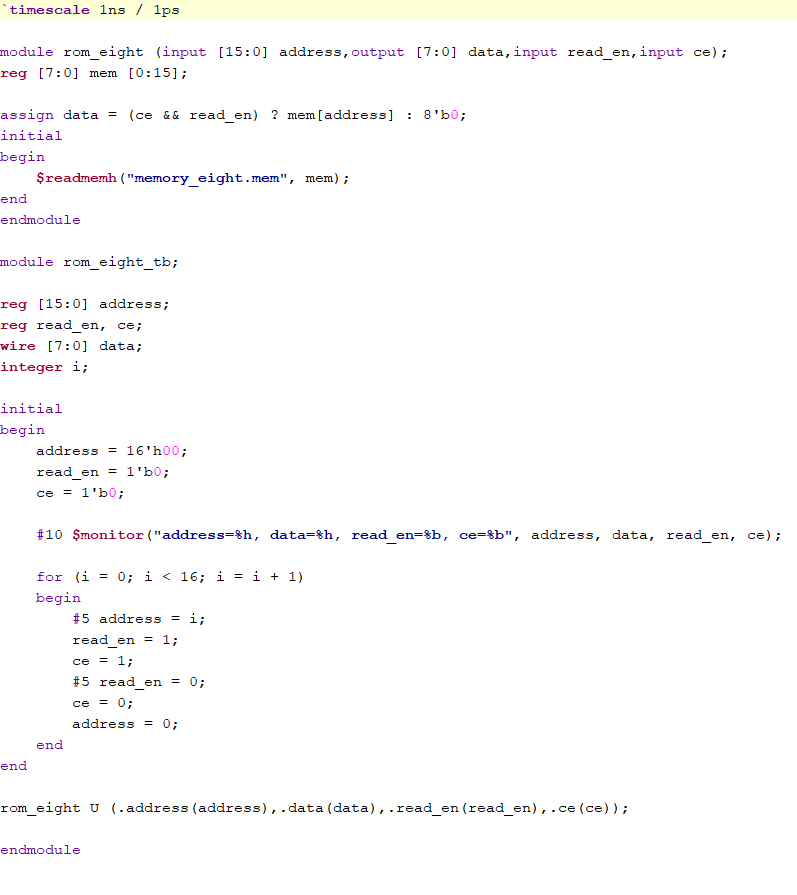
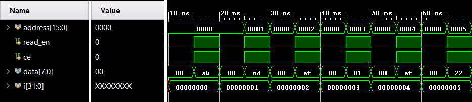
First, an eight bit binary ROM was implemented.
 Figure 8: 8bit binary ROM code and simulation.
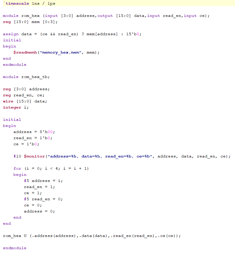
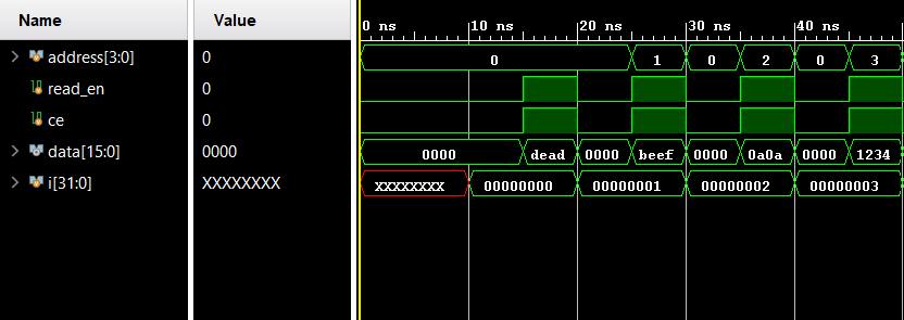
Next, a 16bit hexidecimal ROM was implemented.
Figure 8: 16bit hexidecimal ROM code and simulation.
Next, an 8bit hexidecimal ROM was implemented.
Figure 8: 8bit hexidecimal ROM code and simulation.
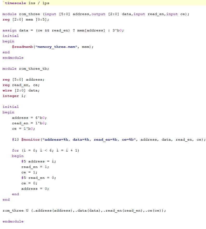
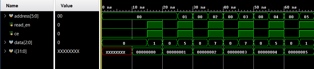
Next, a 3bit binary ROM was implemented.
Figure 8: 3bit binary ROM code and simulation.
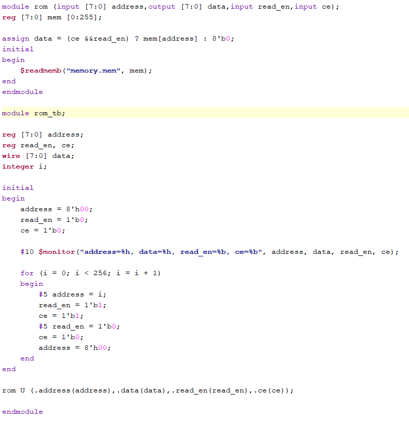
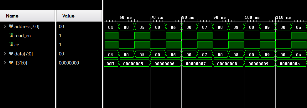
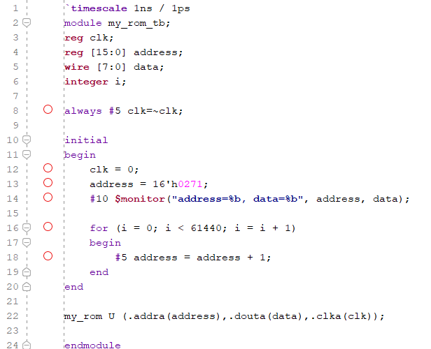
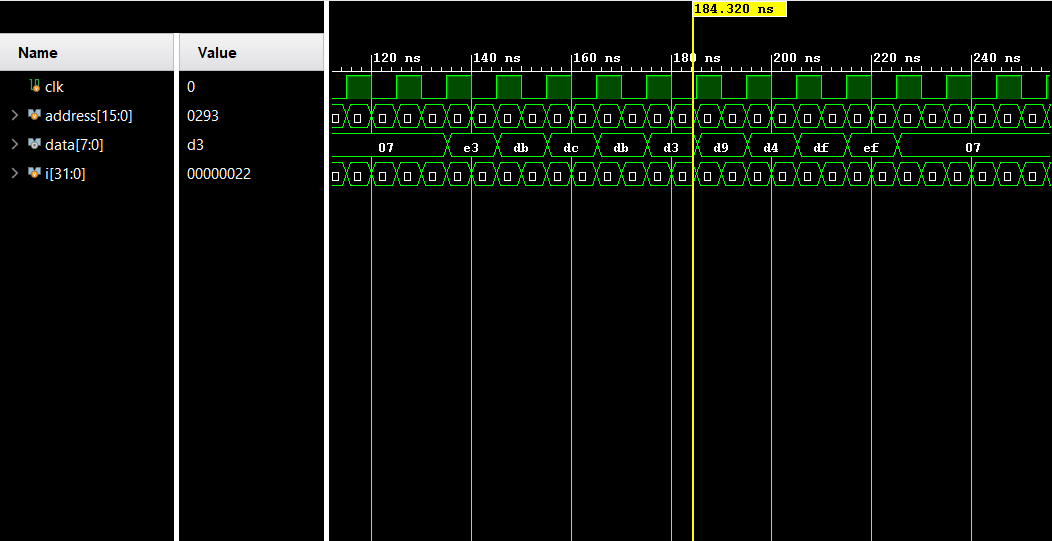
Finally, a ROM IP block was
created and a test bench was designed for it. The address is set with
an offset to demonstrate a change in memory, as all values before
~value 625 decimal are seven.
Figure 8: ROM IP block testbench code and simulation.
Discussion:
This assignment familiarized
me not only with an array of flip-flop designs but also experience
creating memory files and designing a module to read memory files of
different formats. I also gained experience designing a debounce
circuit, then using a virtual implementation later on in the week
during a quiz. Overall, I feel ready to work more with file storage and
memory in Verilog.