This assignment was an in
depth look at more advanced functions in Vivado. This lab started with
binary adders followed by comparators, decoders and encoders,
multiplexer, and finally parity bit modules. While most modules were
simulated virtually, but the two-bit adder, four-one multiplexer, even
parity modules, and the improved modules from homework two were
simulated on the board using switches, leds, and the seven-segment
display.
Task 1:
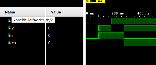
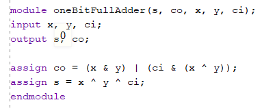
Task one was to recreate half and full one bit adder simulations.
Figure 1: One bit half adder code and simulation
Figure 2: One bit full adder code and simulation
Task 2:
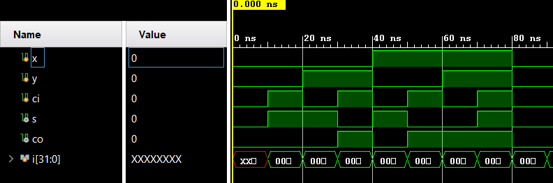
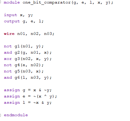
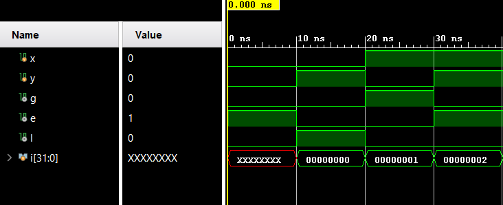
Task two was to design a test bench for a one-bit comparator and run a simulation.
Figure 3: One bit comparator code and simulation.
Task 3:
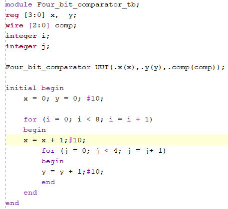
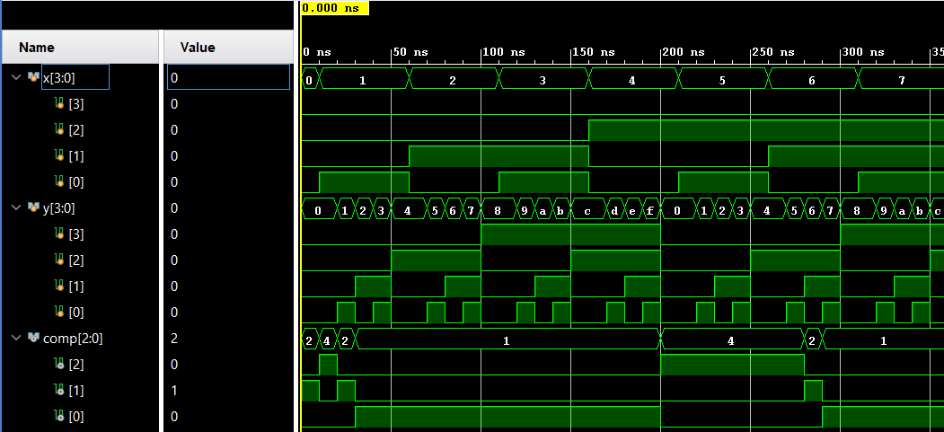
Task three was to design a test bench for a four-bit comparator and run a simulation.
Figure 4: Four bit comparator code and simulation.
Task 4:
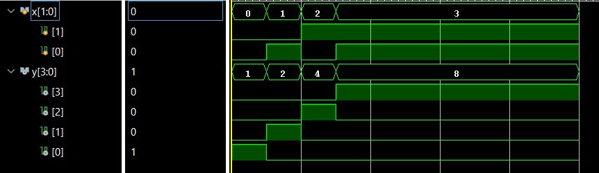
Task four was to implement a two-bit comparator onto the FPGA board using switches as inputs and LEDs as outputs. Figure 5:Two-bit comparator code.
Figure 6: Two-bit comparator FPGA demonstration.
Task 5:
Task five was to design a test bench foor a two-four decoder and run a simulation.
Figure 7: Two-four decoder code and simulation.
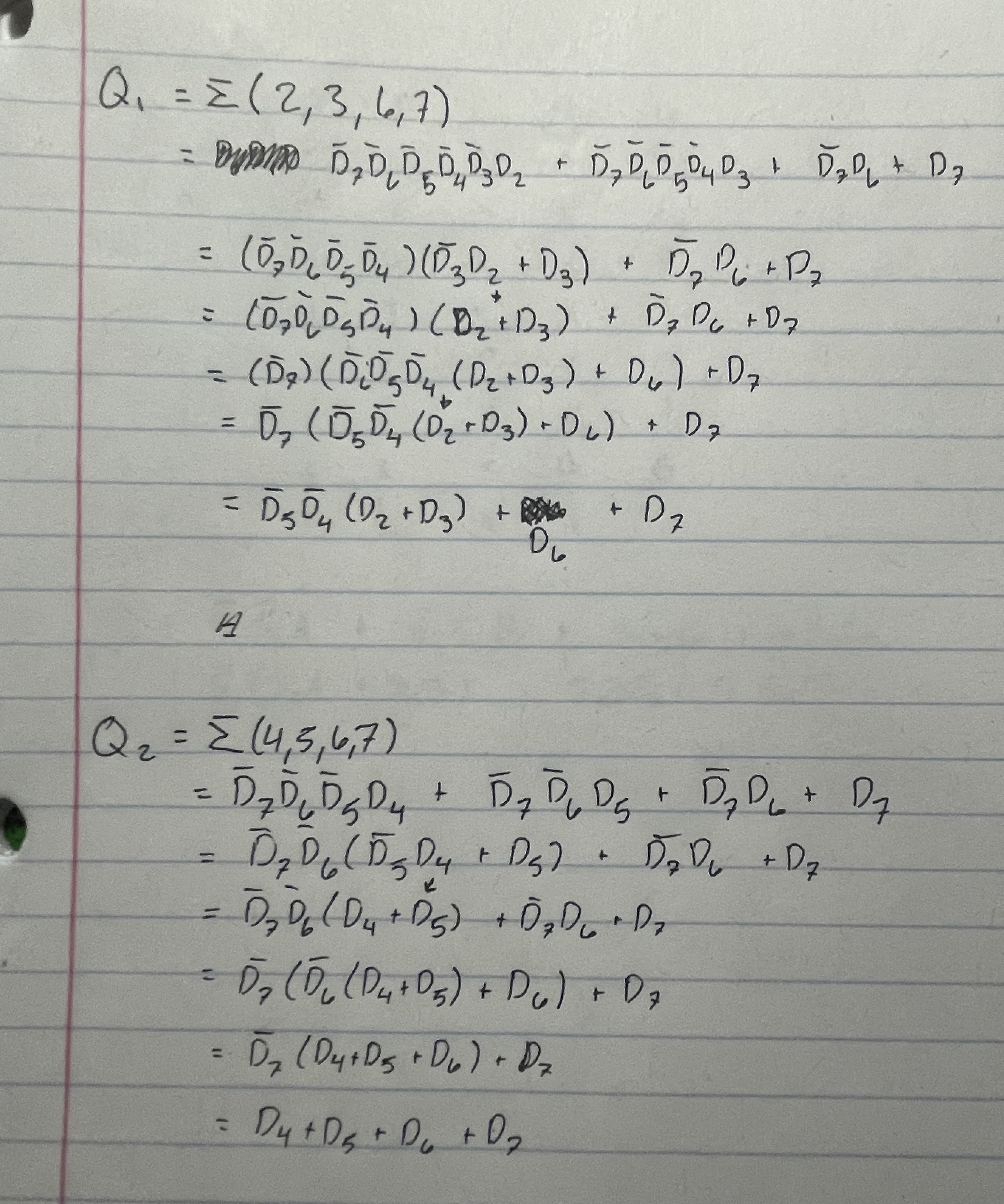
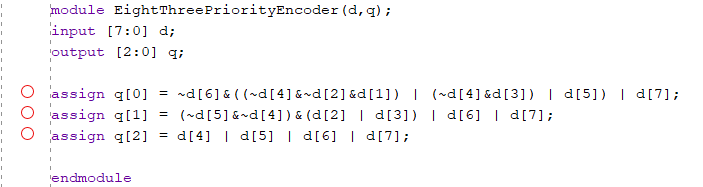
Task 6:
Task six was to finish the
design of a 8x3 priority encoder and run a simulation. One of the
outputs, Q0, was given while the expressions for Q1 and Q2 had to be
found manually. Figure 8: Q1 and Q2 calculations.
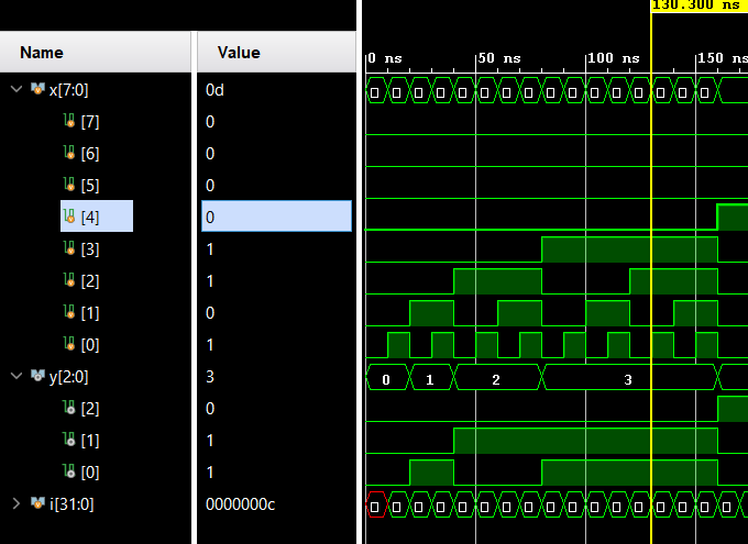
Figure 9:8x3 priority encoder code and simulation.
Task 7:
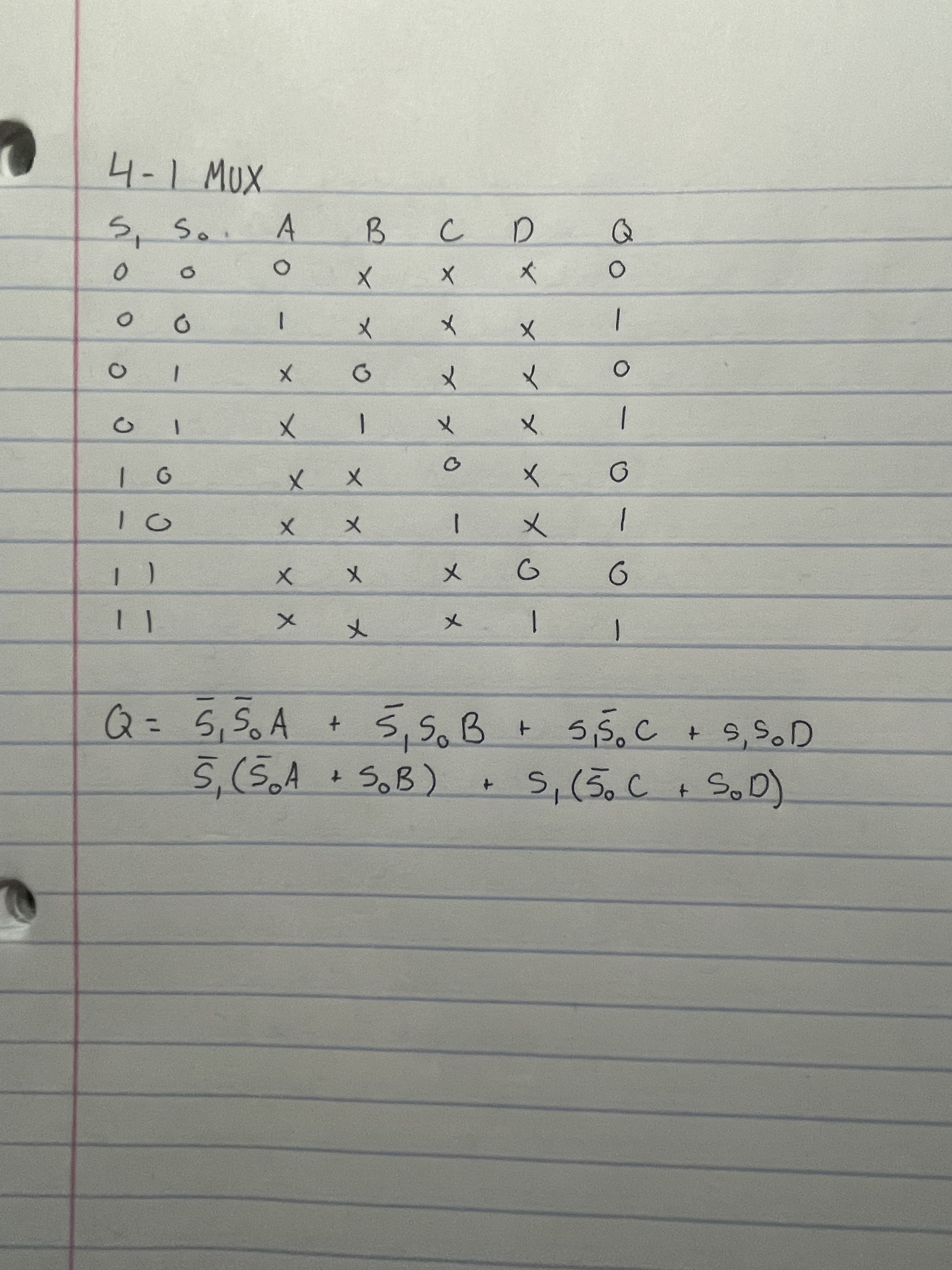
Task seven was to derive the
logical expression for a 4-1 multiplexer, similar to what was required
for the first part of task six. Figure 10: 4-1 multiplexer logic.
Task 8:
Task eight was to implement the 4-1 multiplexer onto the FPGA board to demonstrate functionality of my logic darrived in task 7.
Figure 11: 4-1 multiplexer demonstration.
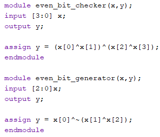
Task 9:
Task nine was to design and implement onto the FPGA board both an even parity generator and checker. Figure 12: Even parity checker code and even parity generator code.
Figure 13: Even parity checker demonstration.
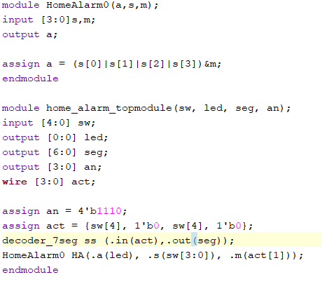
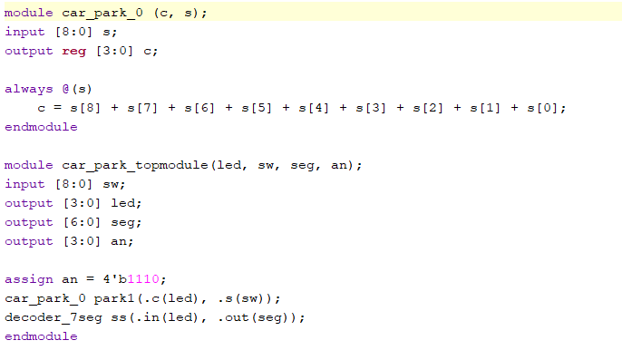
Task 10:
Task ten was to implement
two designs which were both improved versions of the modules created in
homework two: the home alarm module and the parking module. Both
improved versions use a seven-segment display module along with a base
logic module tied together with a head module.
Figure 14: Improved home alarm module code and improved parking module code.
Figure 15: Improved home alarm module demonstration.
Figure 16: Improved parking module demonstration.
Discussion:
This assignment honed my test
bench creating capabilities. I ran into issues often with the
formatting of variables between modules and a greater attention to
detail was required compared to pervious labs. It was also reasuring to
see some of my seven-segment display skills transfer from Lab 3.
Overall, this assignment has forced me to put in hours and familiarize
myself more in depth with Vivado and the FPGA board.